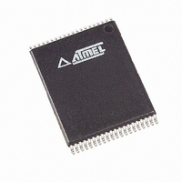
AT49F1024-90VI Atmel, AT49F1024-90VI Datasheet

AT49F1024-90VI
Specifications of AT49F1024-90VI
Related parts for AT49F1024-90VI
AT49F1024-90VI Summary of contents
Page 1
... When the device is deselected, the CMOS standby current is less than 100 µA. The only difference between the AT49F1024 and the AT49F1025 is the package. To allow for simple in-system reprogrammability, the AT49F1024/1025 does not require high-input voltages for programming ...
Page 2
... ADDRESS INPUTS X DECODER READ: The AT49F1024/1025 is accessed like an EPROM. When CE and OE are low and WE is high, the data stored at the memory location determined by the address pins is asserted on the outputs. The outputs are put in the high impedance state whenever high. This dual line control gives designers flexibility in preventing bus contention ...
Page 3
... For details, see Operating Modes (for hardware operation) or Software Product Identifi- cation. The manufacturer and device code is the same for both modes. DATA POLLING: The AT49F1024/1025 features Data Polling to indicate the end of a program or erase cycle. During a program cycle, an attempted read of the last byte loaded will result in the complement of the loaded data on I/O7 ...
Page 4
... Temperature under Bias ................................ -55°C to +125°C Storage Temperature ..................................... -65°C to +150°C All Input Voltages (including NC Pins) with Respect to Ground ...................................-0.6V to +6.25V All Output Voltages with Respect to Ground .............................-0. Voltage on OE with Respect to Ground ...................................-0.6V to +13.5V AT49F1024/1025 4 1st Bus 2nd Bus 3rd Bus Cycle Cycle Cycle Data ...
Page 5
... Condition MHz OUT -400 µ -100 µ 4. AT49F1024/1025 AT49F1024-55 AT49F1024-50 AT49F1025-55 0°C - 70°C 0°C - 70°C -40°C - 85°C 5V ± 10% 5V ± 10 High-Z High-Z ( A15 = Manufacturer Code ( A15 = Device Code A15 = V Manufacturer Code A15 = V Device Code IH IL Min Max 10.0 10 ...
Page 6
... AT49F1024-45 AT49F1025-35 AT49F1025-45 AT49F1024-50 Min Max Min Max Min after the address transition without impact on t ACC after the falling edge of CE without impact pF). L AT49F1024-55 AT49F1024-70 AT49F1025-55 AT49F1025-70 Max Min Max Min ACC after an address change CE ACC OE Max Units 70 ns ...
Page 7
... Input Test Waveforms and Measurement Level Output Test Load Pin Capacitance ( MHz 25°C Symbol Typ OUT Note: 1. This parameter is characterized and is not 100% tested. 0765I–05/ < 5.0V 1.8K OUTPUT PIN 30 pF 1.3K Max 6 12 AT49F1024/1025 Units Conditions OUT 7 ...
Page 8
... Chip Select Setup Time CS t Chip Select Hold Time CH t Write Pulse Width ( Data Setup Time Data, OE Hold Time DH OEH t Write Pulse Width High WPH AC Word Load Waveforms WE Controlled OE ADDRESS CE WE DATA IN CE Controlled OE ADDRESS WE CE DATA IN AT49F1024/1025 OES OES Min Max ...
Page 9
... OE must be high only when WE and CE are both low. 2. For chip erase, the address should be 10H. For a main memory erase, the data should be 30H. 0765I–05/ WPH 5555 2AAA 5555 5555 WORD 0 WORD 1 WORD 2 AT49F1024/1025 Min Typ 2AAA 5555 NOTE 2 WORD 3 WORD 4 WORD 5 Max Units 50 µ ...
Page 10
... Read Characteristics” on page 6. OE (1)(2)(3) Toggle Bit Waveforms Notes: 1. Toggling either both OE and CE will operate toggle bit. The t input(s). 2. Beginning and ending state of I/O6 will vary. 3. Any address location may be used but the address should not vary. AT49F1024/1025 10 (1) (1) Min Typ Max 10 10 ...
Page 11
... ADDRESS 2AAA LOAD DATA 90 TO ADDRESS 5555 ENTER PRODUCT IDENTIFICATION (2)(3)(5) MODE (1) OR LOAD DATA AA TO ADDRESS 5555 LOAD DATA 55 IDENTIFICATION TO ADDRESS 2AAA LOAD DATA F0 TO ADDRESS 5555 EXIT PRODUCT IDENTIFICATION (4) MODE . AT49F1024/1025 LOAD DATA F0 TO ANY ADDRESS EXIT PRODUCT (4) MODE 11 ...
Page 12
... Boot Block Lockout Enable Algorithm Notes: 1. Data Format: I/O15 - I/O8 (Don’t Care); I/O7 - I/O0 (Hex). Address Format: A15 - A0 (Hex); A15 (Don’t Care). 2. Boot Block Lockout feature enabled. AT49F1024/1025 12 (1) LOAD DATA AA TO ADDRESS 5555 LOAD DATA 55 TO ADDRESS 2AAA ...
Page 13
... AT49F1024 Ordering Information I (mA ACC (ns) Active Standby 0 0.1 50 0.3 AT49F1025 Ordering Information I (mA ACC (ns) Active Standby 0 0.1 50 0.3 44J 44-lead, Plastic J-leaded Chip Carrier Package (PLCC) 40V 40-lead mm, Thin Small Outline Package (VSOP) 0765I– ...
Page 14
... IDENTIFY .656(16.7) .650(16.5) .032(.813) .695(17.7) .026(.660) .685(17.4) .050(1.27) TYP .500(12.7) REF SQ .022(.559) X 45° MAX (3X) AT49F1024/1025 14 40V, 40-lead, Plastic Thin Small Outline Package (VSOP) Dimensions in Millimeters and (Inches)* .045(1.14) X 30° - 45° .012(.305) .008(.203) .630(16.0) SQ .590(15.0) ...
Page 15
... No licenses to patents or other intellectual property of Atmel are granted by the Company in connection with the sale of Atmel products, expressly or by implication. Atmel’s products are not authorized for use as critical components in life support devices or systems. ...


