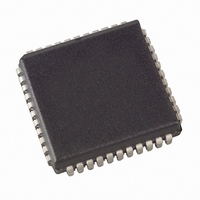
AT49F1025-70JI Atmel, AT49F1025-70JI Datasheet

AT49F1025-70JI
Specifications of AT49F1025-70JI
Available stocks
Related parts for AT49F1025-70JI
AT49F1025-70JI Summary of contents
Page 1
... Typical 10,000 Write Cycles Description The AT49F1024 and the AT49F1025 are 5-volt-only in-system Flash memories. Their 1 megabit of memory is organized as 65,536 words by 16 bits. Manufactured with Atmel’s advanced nonvolatile CMOS technology, the devices offer access times with power dissipation of just 275 mW over the commercial temperature range. ...
Page 2
... The Main Memory Erase command is a six-bus cycle operation. The address (5555H) is latched on the falling edge of the sixth cycle while the 30H data input is latched on the rising edge of WE. The main memory erase starts after the rising edge the sixth cycle. Please see main memory erase cycle waveforms. The main memory erase operation is internally controlled ...
Page 3
... The software product identification exit code should be used to return to standard operation. PRODUCT IDENTIFICATION: The product identification mode identifies the device and manufacturer as Atmel. It may be accessed by hardware or software operation. The hardware operation mode can be used by an external programmer to identify the correct programming algorithm for the Atmel product. ...
Page 4
... Command Definition (in Hex) Command Bus Sequence Cycles Addr Read 1 Addr Chip Erase 6 5555 Main Memory Erase 6 5555 Word Program 4 5555 (2) Boot Block Lockout 6 5555 Product ID Entry 3 5555 (3) Product ID Exit 3 5555 (3) Product ID Exit 1 xxxx Notes: 1. The DATA FORMAT in each bus cycle is as follows: I/O15 - I/O8 (Don’t Care); I/O7 - I/O0 (Hex). ...
Page 5
... A15 = Device Code A15 = V Manufacturer Code A15 = V Device Code IH IL Min Max 10.0 10.0 Com. 100.0 Ind. 300.0 3.0 50.0 0.8 2.0 0.45 2.4 4.2 AT49F1024-70 AT49F1025-70 0°C - 70°C -40°C - 85°C 5V ± 10% OUT IN (4) (4) (4) (4) Units µA µA µA µ ...
Page 6
... AT49F1024-35 AT49F1024-45 AT49F1025-35 AT49F1025-45 AT49F1024-50 Min Max Min Max Min after the address transition without impact on t ACC after the falling edge of CE without impact pF). L AT49F1024-55 AT49F1024-70 AT49F1025-55 AT49F1025-70 Max Min Max Min ACC after an address change CE ACC OE Max Units ...
Page 7
Input Test Waveforms and Measurement Level Output Test Load Pin Capacitance ( MHz 25°C Symbol Typ OUT Note: 1. This parameter is characterized and is not 100% tested. 0765I–05/01 t ...
Page 8
AC Word Load Characteristics Symbol Parameter Address, OE Setup Time AS OES t Address Hold Time AH t Chip Select Setup Time CS t Chip Select Hold Time CH t Write Pulse Width (WE or CE) WP ...
Page 9
... Program Cycle Waveforms A0-A15 Main Memory or Chip Erase Cycle Waveforms A0-A15 DATA Notes must be high only when WE and CE are both low. 2. For chip erase, the address should be 10H. For a main memory erase, the data should be 30H. 0765I–05/ WPH 5555 2AAA ...
Page 10
Data Polling Characteristics Symbol Parameter t Data Hold Time Hold Time OEH ( Output Delay OE t Write Recovery Time WR Notes: 1. These parameters are characterized and not 100% tested. 2. See t ...
Page 11
Software Product Identification Entry Software Product Identification Exit Notes: 1. Data Format: I/O15 - I/O8 (Don’t Care); I/O7 - I/O0 (Hex). Address Format: A15 - A0 (Hex); A15 (Don’t Care A15 = Manufacturer Code ...
Page 12
Boot Block Lockout Enable Algorithm Notes: 1. Data Format: I/O15 - I/O8 (Don’t Care); I/O7 - I/O0 (Hex). Address Format: A15 - A0 (Hex); A15 (Don’t Care). 2. Boot Block Lockout feature enabled. AT49F1024/1025 12 (1) LOAD DATA AA TO ...
Page 13
... AT49F1024-70VI 40V Ordering Code Package AT49F1025-35JC 44J AT49F1025-45JC 44J AT49F1025-55JC 44J AT49F1025-55JI 44J AT49F1025-70JC 44J AT49F1025-70JI 44J Package Type AT49F1024/1025 Operation Range Commercial (0° to 70°C) Commercial (0° to 70°C) Commercial (0° to 70°C) Commercial (0° to 70°C) Industrial (-40° to 85°C) Commercial (0° ...
Page 14
Packaging Information 44J, 44-lead, Plastic J-leaded Chip Carrier (PLCC) Dimensions in Inches and (Millimeters) JEDEC STANDARD MS-018 AC .045(1.14) X 45° PIN NO. 1 IDENTIFY .656(16.7) .650(16.5) .032(.813) .695(17.7) .026(.660) .685(17.4) .050(1.27) TYP .500(12.7) REF SQ .022(.559) X 45° MAX ...
Page 15
... No licenses to patents or other intellectual property of Atmel are granted by the Company in connection with the sale of Atmel products, expressly or by implication. Atmel’s products are not authorized for use as critical components in life support devices or systems. ...


