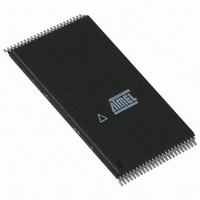
AT49BV1614-90TC Atmel, AT49BV1614-90TC Datasheet - Page 5

AT49BV1614-90TC
Manufacturer Part Number
AT49BV1614-90TC
Description
IC FLASH 16MBIT 90NS 48TSOP
Manufacturer
Atmel
Datasheet
1.AT49BV1604-11UI.pdf
(18 pages)
Specifications of AT49BV1614-90TC
Format - Memory
FLASH
Memory Type
FLASH
Memory Size
16M (2M x 8 or 1M x 16)
Speed
90ns
Interface
Parallel
Voltage - Supply
3 V ~ 3.6 V
Operating Temperature
0°C ~ 70°C
Package / Case
48-TSOP
Lead Free Status / RoHS Status
Contains lead / RoHS non-compliant
Suspend feature while erasing a sector when you want to
read data from a sector in the other plane. After the Erase
Suspend command is given, the device requires a maxi-
mum time of 15 µs to suspend the erase operation. After
the erase operation has been suspended, the plane that
contains the suspended sector enters the erase-suspend-
read mode. The system can then read data or program
data to any other sector within the device. An address is
not required during the Erase Suspend command. During a
sector erase suspend, another sector cannot be erased. To
resume the sector erase operation, the system must write
the Erase Resume command. The Erase Resume com-
mand is a one-bus cycle command, which does require the
plane address (determined by A18 and A19). The device
also supports an erase suspend during a complete chip
erase. While the chip erase is suspended, the user can
read from any sector within the memory that is protected.
The command sequence for a chip erase suspend and a
sector erase suspend are the same.
PRODUCT IDENTIFICATION: The product identification
mode identifies the device and manufacturer as Atmel. It
may be accessed by hardware or software operation. The
hardware operation mode can be used by an external pro-
grammer to identify the correct programming algorithm for
the Atmel product.
For details, see “Operating Modes” on page 9 (for hard-
ware operation) or “Software Product Identification
Entry/Exit” on page 14. The manufacturer and device code
is the same for both modes.
DATA POLLING: The AT49BV16X4(T) features Data Poll-
ing to indicate the end of a program cycle. During a
program cycle an attempted read of the last byte/word
loaded will result in the complement of the loaded data on
I/O7. Once the program cycle has been completed, true
data is valid on all outputs and the next cycle may begin.
During a chip or sector erase operation, an attempt to read
the device will give a “0” on I/O7. Once the program or
erase cycle has completed, true data will be read from the
device. Data Polling may begin at any time during the pro-
gram cycle. Please see “Status Bit Table” on page 15 for
more details.
T O G G L E B I T : I n a d d i t i o n t o D a t a P o l l i n g , t h e
AT49BV16X4(T) provides another method for determining
the end of a program or erase cycle. During a program or
erase operation, successive attempts to read data from the
same memory plane will result in I/O6 toggling between
one and zero. Once the program cycle has completed, I/O6
will stop toggling and valid data will be read. Examining the
toggle bit may begin at any time during a program cycle.
An additional toggle bit is available on I/O2, which can be
used in conjunction with the toggle bit that is available on
I/O6. While a sector is erase suspended, a read or a pro-
gram operation from the suspended sector will result in the
I/O2 bit toggling. Please see “Status Bit Table” on page 15
for more details.
RDY/BUSY: An open drain Ready/Busy output pin pro-
vides another method of detecting the end of a program or
erase operation. RDY/BUSY is actively pulled low during
the internal program and erase cycles and is released at
the completion of the cycle. The open drain connection
allows for OR-tying of several devices to the same
RDY/BUSY line.
HARDWARE DATA PROTECTION: The Hardware Data
Protection feature protects against inadvertent programs to
the AT49BV16X4(T) in the following ways: (a) V
V
ited. (b) V
V
10 ms (typical) before programming. (c) Program inhibit:
holding any one of OE low, CE high or WE high inhibits
program cycles. (d) Noise filter: pulses of less than 15 ns
(typical) on the WE or CE inputs will not initiate a program
cycle.
INPUT LEVELS: While operating with a 2.7V to 3.6V
power supply, the address inputs and control inputs (OE,
CE and WE) may be driven from 0 to 5.5V without
adversely affecting the operation of the device. The I/O
lines can only be driven from 0 to V
OUTPUT LEVELS: For the 49BV1604(T), output high
levels (V
3.6V output levels, V
2.2V output levels, V
while V
power).
CC
CC
is below 1.8V (typical), the program function is inhib-
sense level, the device will automatically time out
CC
OH
CC
must be regulated to 2.7V - 3.0V (for minimum
) are equal to V
power-on delay: once V
CCQ
CCQ
must be regulated to 2.0V ± 10%,
must be tied to V
CCQ
- 0.2V (not V
CC
+ 0.6V.
CC
has reached the
CC
CC
). For 2.7V -
. For 1.8V -
CC
sense: if
5


