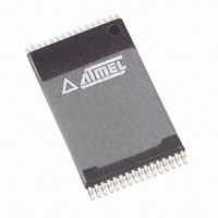
AT49BV002AT-70VI Atmel, AT49BV002AT-70VI Datasheet

AT49BV002AT-70VI
Specifications of AT49BV002AT-70VI
Available stocks
Related parts for AT49BV002AT-70VI
AT49BV002AT-70VI Summary of contents
Page 1
... AT49BV002A(T), once the boot block programming lockout feature is enabled, the contents of the boot block cannot be changed with input voltage levels of 5.5 volts or less. 2-megabit (256K x 8) Single 2.7-volt Battery-Voltage Flash Memory AT49BV002A AT49BV002AN AT49BV002AT AT49BV002ANT Not Recommended for New Design 3353G–FLASH–8/05 ...
Page 2
Pin Configurations Pin Name A0 - A17 RESET I/O0 - I/O7 2.1 32-lead PLCC Top View 2.2 32-lead VSOP ( mm) or 32-lead TSOP, Type mm) Top View Note: AT49BV002A(N)(T) ...
Page 3
... Read The AT49BV002A(N)(T) is accessed like an EPROM. When CE and OE are low and WE is high, the data stored at the memory location determined by the address pins is asserted on the out- puts. The outputs are put in the high impedance state whenever high. This dual-line control gives designers flexibility in preventing bus contention. ...
Page 4
... If the boot block lockout has been enabled, the Chip Erase function will erase Parameter Block 1, Parameter Block 2, Main Memory Block but not the boot block. If the Boot Block Lockout has not been enabled, the Chip Erase function will erase the entire chip. After the full chip erase the device will return back to read mode ...
Page 5
... AT49BV002AN(T). 4.7 Product Identification The product identification mode identifies the device and manufacturer as Atmel. It may be accessed by hardware or software operation. The hardware operation mode can be used by an external programmer to identify the correct programming algorithm for the Atmel product. ...
Page 6
DATA Polling The AT49BV002A(N)(T) features DATA polling to indicate the end of a program cycle. During a program cycle an attempted read of the last byte loaded will result in the complement of the loaded data on I/O7. Once ...
Page 7
... SA = 3A000 to 3BFFF for PARAMETER BLOCK 38000 to 39FFF for PARAMETER BLOCK 30000 to 37FFF for MAIN MEMORY ARRAY BLOCK 20000 to 2FFFF for MAIN MEMORY ARRAY BLOCK 10000 to 1FFFF for MAIN MEMORY ARRAY BLOCK 00000 to 0FFFF for MAIN MEMORY ARRAY BLOCK 4 6. Absolute Maximum Ratings* Temperature Under Bias ............................... -55° ...
Page 8
DC and AC Operating Range Operating Temperature (Case) V Power Supply CC 8. Operating Modes Mode CE Read V IL (2) Program/Erase V IL Standby/Write Inhibit V IH Program Inhibit X Program Inhibit X Output Disable X Reset X ...
Page 9
AC Read Characteristics Symbol Parameter t Address to Output Delay ACC ( Output Delay CE ( Output Delay OE (3)( Output Float DF Output Hold from OE, CE ...
Page 10
Input Test Waveform and Measurement Level DRIVING LEVELS < 13. Output Load Test 14. Pin Capacitance ( MHz 25°C Symbol Typ OUT ...
Page 11
AC Byte Load Characteristics Symbol Parameter Address, OE Set-up Time AS OES t Address Hold Time AH t Chip Select Set-up Time CS t Chip Select Hold Time CH t Write Pulse Width (WE or CE) ...
Page 12
Program Cycle Characteristics Symbol Parameter t Byte Programming Time BP t Address Set-up Time AS t Address Hold Time AH t Data Set-up Time DS t Data Hold Time DH t Write Pulse Width WP t Write Pulse Width ...
Page 13
Data Polling Characteristics Symbol Parameter t Data Hold Time Hold Time OEH ( Output Delay OE t Write Recovery Time WR Notes: 1. These parameters are characterized and not 100% tested. 2. See ...
Page 14
Software Product Identification (1) Entry LOAD DATA AA TO ADDRESS 555 LOAD DATA 55 TO ADDRESS AAA LOAD DATA 90 TO ADDRESS 555 ENTER PRODUCT IDENTIFICATION (2)(3)(5) MODE 25. Software Product Identification (1) Exit OR LOAD DATA AA TO ...
Page 15
... Ordering Code Package AT49BV002A-70JI 32J AT49BV002A-70TI 32T AT49BV002A-70VI 32V AT49BV002AN-70JI 32J AT49BV002AN-70TI 32T AT49BV002AN-70VI 32V AT49BV002AT-70JI 32J AT49BV002AT-70TI 32T AT49BV002AT-70VI 32V AT49BV002ANT-70JI 32J AT49BV002ANT-70TI 32T AT49BV002ANT-70VI 32V Ordering Code Package AT49BV002AN-70JU 32J AT49BV002AN-70TU 32T AT49BV002AN-70VU 32V AT49BV002ANT-70JU 32J AT49BV002ANT-70TU ...
Page 16
Packaging Information 28.1 32J – PLCC 1.14(0.045 0.51(0.020)MAX 45 MAX (3X) Notes: 1. This package conforms to JEDEC reference MS-016, Variation AE. 2. Dimensions D1 and E1 do not include mold protrusion. Allowable protrusion is ...
Page 17
TSOP Pin 1 Identifier e E Notes: 1. This package conforms to JEDEC reference MO-142, Variation BD. 2. Dimensions D1 and E do not include mold protrusion. Allowable protrusion 0.15 mm per side and ...
Page 18
VSOP Pin 1 Identifier e E Notes: 1. This package conforms to JEDEC reference MO-142, Variation BA. 2. Dimensions D1 and E do not include mold protrusion. Allowable protrusion 0.15 mm per side and ...
Page 19
... Disclaimer: The information in this document is provided in connection with Atmel products. No license, express or implied, by estoppel or otherwise, to any intellectual property right is granted by this document or in connection with the sale of Atmel products. EXCEPT AS SET FORTH IN ATMEL’S TERMS AND CONDI- TIONS OF SALE LOCATED ON ATMEL’S WEB SITE, ATMEL ASSUMES NO LIABILITY WHATSOEVER AND DISCLAIMS ANY EXPRESS, IMPLIED OR STATUTORY WARRANTY RELATING TO ITS PRODUCTS INCLUDING, BUT NOT LIMITED TO, THE IMPLIED WARRANTY OF MERCHANTABILITY, FITNESS FOR A PARTICULAR PURPOSE, OR NON-INFRINGEMENT ...


