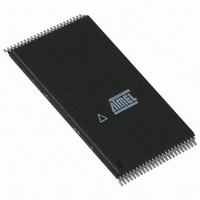
AT49BV1614-90TI Atmel, AT49BV1614-90TI Datasheet - Page 2

AT49BV1614-90TI
Manufacturer Part Number
AT49BV1614-90TI
Description
IC FLASH 16MBIT 90NS 48TSOP
Manufacturer
Atmel
Datasheets
1.AT49BV1604-90TI.pdf
(18 pages)
2.AT49BV1604-90TI.pdf
(18 pages)
3.AT49BV1614-90TI.pdf
(18 pages)
Specifications of AT49BV1614-90TI
Format - Memory
FLASH
Memory Type
FLASH
Memory Size
16M (2M x 8 or 1M x 16)
Speed
90ns
Interface
Parallel
Voltage - Supply
3 V ~ 3.6 V
Operating Temperature
-40°C ~ 85°C
Package / Case
48-TSOP
Lead Free Status / RoHS Status
Contains lead / RoHS non-compliant
contention. This device can be read or reprogrammed
using a single 2.7V power supply, making it ideally suited
for in-system programming.
The device powers on in the read mode . Command
sequences are used to place the device in other operation
modes such as program and erase. The device has the
capability to protect the data in any sector. Once the data
protection for a given sector is enabled, the data in that
sector cannot be changed using input levels between
ground and V
The device is segmented into two memory planes. Reads
from memory plane B may be performed even while
2
RESET
RDY/BUSY
VPP
A15
A14
A13
A12
A11
A10
A19
A18
A17
WE
NC
NC
NC
A9
A8
A7
A6
A5
A4
A3
A2
A1
RESET
VPP
A15
A14
A13
A12
A11
A10
A19
A18
A17
WE
NC
NC
A9
A8
A7
A6
A5
A4
A3
A2
A1
1
2
3
4
5
6
7
8
9
10
11
12
13
14
15
16
17
18
19
20
21
22
23
24
1
2
3
4
5
6
7
8
9
10
11
12
13
14
15
16
17
18
19
20
21
22
23
24
CC
.
TSOP Top View
TSOP Top View
Type 1
Type 1
AT49BV1604(T)/1614(T)
48
47
46
45
44
43
42
41
40
39
38
37
36
35
34
33
32
31
30
29
28
27
26
25
48
47
46
45
44
43
42
41
40
39
38
37
36
35
34
33
32
31
30
29
28
27
26
25
A16
BYTE
GND
I/O15/A-1
I/O7
I/O14
I/O6
I/O13
I/O5
I/O12
I/O4
VCC
I/O11
I/O3
I/O10
I/O2
I/O9
I/O1
I/O8
I/O0
OE
GND
CE
A0
A16
VCCQ
GND
I/O15
I/O7
I/O14
I/O6
I/O13
I/O5
I/O12
I/O4
VCC
I/O11
I/O3
I/O10
I/O2
I/O9
I/O1
I/O8
I/O0
OE
GND
CE
A0
AT49BV1604(T)
AT49BV1614(T)
program or erase functions are being executed in memory
plane A and vice versa. This operation allows improved
system performance by not requiring the system to wait for
a program or erase operation to complete before a read is
performed. To further increase the flexibility of the device, it
contains an Erase Suspend feature. This feature will put
the Erase on hold for any amount of time and let the user
read data from or program data to any of the remaining
sectors within the same memory plane. There is no reason
to suspend the erase operation if the data to be read is in
the other memory plane. The end of a program or an Erase
cycle is detected by the Ready/Busy pin, Data polling, or by
the toggle bit.
C
D
A
B
E
F
G
C
D
H
A
B
E
F
VCCQ
GND
A13
A14
A15
A16
1
µBGA Top View (Ball Down)
I/O14
I/O15
A11
A10
A12
I/O7
2
VSS
CE
OE
A3
A4
A2
A1
A0
1
I/O13
I/O5
I/O6
CBGA Top View
WE
A8
A9
3
A17
I/O0
I/O8
I/O9
I/O1
A7
A6
A5
2
RDY/BUSY
I/O11
I/O12
VPP
RST
I/O4
4
I/O10
I/O11
I/O2
I/O3
A18
NC
NC
3
VCC
A18
I/O2
I/O3
RESET
5
I/O12
VCC
VPP
I/O5
I/O4
WE
A19
4
I/O10
A19
A17
I/O8
I/O9
A6
6
I/O14
I/O13
I/O7
I/O6
A10
A11
A9
A8
5
I/O0
I/O1
CE
A7
A5
A3
7
BYTE
I/O15
VSS
A13
A12
A14
A15
A16
/A-1
6
GND
OE
8
A4
A2
A1
A0


