AT25256A-10TU-2.7 Atmel, AT25256A-10TU-2.7 Datasheet
AT25256A-10TU-2.7
Specifications of AT25256A-10TU-2.7
AT25AT256A-10TU-2.7 SL383
Available stocks


Related parts for AT25256A-10TU-2.7


AT25256A-10TU-2.7 Summary of contents
Page 1
... TSSOP 1 8 VCC HOLD SCK GND 4 5 8-ball dBGA2 VCC HOLD SCK 4 GND 5 4 GND S I Bottom View SPI Serial EEPROMs 128K (16,384 x 8) 256K (32,768 x 8) AT25128A AT25256A Not Recommended for New Design VCC HOLD SCK SI 3368J–SEEPR–06/07 ...
Page 2
Table 0-1. Pin Configurations Pin Name Function CS Chip Select SCK Serial Data Clock SI Serial Data Input SO Serial Data Output GND Ground VCC Power Supply WP Write Protect HOLD Suspends Serial Input NC No Connect Block Write protection ...
Page 3
Figure 1-1. Block Diagram (1) Table 1-1. Pin Capacitance Applicable over recommended operating range from T Symbol Test Conditions C Output Capacitance (SO) OUT C Input Capacitance (CS, SCK, SI, WP, HOLD) IN Note: 1. This parameter is characterized and ...
Page 4
Table 1-2. DC Characteristics Applicable over recommended operating range from T 40C to +125 +1.8V to +5.5V(unless otherwise noted Symbol Parameter V Supply Voltage CC1 V Supply Voltage CC2 V Supply Voltage CC3 ...
Page 5
Table 1-3. AC Characteristics Applicable over recommended operating range from TTL Gate and 30 pF (unless otherwise noted) Symbol Parameter f SCK Clock Frequency SCK t Input Rise Time RI t Input Fall Time FI t ...
Page 6
... Hold to Output High Output Disable Time DIS t Write Cycle Time WC (1) Endurance 5.0V, 25C, Page Mode Notes: 1. This parameter is characterized and is not 100% tested. Contact Atmel for further information. AT25128A_256A 6 = 40 85 40C to +125 Voltage Min 4.55.5 2.7 ...
Page 7
Serial Interface Description MASTER: The device that generates the serial clock. SLAVE: Because the serial clock pin (SCK) is always an input, the AT25128A/256A always operates as a slave. TRANSMITTER/RECEIVER: The AT25128A/256A has separate pins designated for data transmission ...
Page 8
Figure 2-1. SPI Serial Interface AT25128A_256A 8 AT25128A/256A 3368J–SEEPR–06/07 ...
Page 9
... Set Write Enable Latch 0000 X100 Reset Write Enable Latch 0000 X101 Read Status Register 0000 X001 Write Status Register 0000 X011 Read Data from Memory Array 0000 X010 Write Data to Memory Array Status Register Format Bit 6 Bit 5 Bit 4 Bit BP1 ...
Page 10
... Protected Low 1 Protected High 0 Protected High 1 Protected 3-4. , RDSR). WC Array Addresses Protected AT25128A AT25256A None None 3000 – 3FFF 6000 – 7FFF 2000 – 3FFF 4000 – 7FFF 0000 – 3FFF 0000 – 7FFF Unprotected Status Blocks Register Protected Protected Writable ...
Page 11
... CS is brought high. A new CS falling edge is required to re-initiate the serial communication. Table 3-6. 3368J–SEEPR–06/07 Table 3-6). Programming will start after the CS pin is brought Address Key Address AT25128A A N Don’t Care Bits AT25128A_256A AT25256A A ...
Page 12
Timing Diagrams (for SPI Mode 0 (0, 0)) Figure 4-1. Synchronous Data Timing CSS V IH SCK HI Figure ...
Page 13
Figure 4-3. WRDI Timing Figure 4-4. RDSR Timing CS 0 SCK SI INSTRUCTION HIGH IMPEDANCE SO Figure 4-5. WRSR Timing 3368J–SEEPR–06/ MSB AT25128A_256A ...
Page 14
Figure 4-6. READ Timing Figure 4-7. WRITE Timing Figure 4-8. HOLD Timing CS SCK HOLD SO AT25128A_256A 3368J–SEEPR–06/07 ...
Page 15
AT25128A Ordering Information Ordering Code (2) AT25128A-10PU-2.7 (2) AT25128A-10PU-1.8 (2) AT25128AN-10SU-2.7 (2) AT25128AN-10SU-1.8 (2) AT25128AW-10SU-2.7 (2) AT25128AW-10SU-1.8 (2) AT25128A-10TU-2.7 (2) AT25128A-10TU-1.8 (2) AT25128AU2-10UU-1.8 (2) AT25128AY7-10YH-1.8 (3) AT25128A-W1.8-11 Notes: 1. For 2.7V devices used in the 4.5V to 5.5V range, ...
Page 16
... AT25256A-10PU-2.7 (2) AT25256A-10PU-1.8 (2) AT25256AN-10SU-2.7 (2) AT25256AN-10SU-1.8 (2) AT25256AW-10SU-2.7 (2) AT25256AW-10SU-1.8 (2) AT25256A-10TU-2.7 (2) AT25256A-10TU-1.8 (2) AT25256AU2-10UU-1.8 (2) AT25256AY7-10YH-1.8 (3) AT25256A-W1.8-11 Notes: 1. For 2.7V devices used in the 4.5V to 5.5V range, please refer to performance values in the AC and DC Characteristics tables. 2. “U” designates Green package + RoHS compliant. 3. Available in waffle pack and wafer form; order as SL788 for wafer form. Bumped die available upon request. Please contact Serial Interface Marketing ...
Page 17
Packaging Information 8P3 – PDIP Top View PLCS Side View Notes: 1. This drawing is for general information only; refer to JEDEC Drawing MS-001, Variation BA, for additional information. 2. Dimensions A and L are ...
Page 18
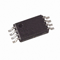
JEDEC SOIC TOP VIEW TOP VIEW e e SIDE VIEW SIDE VIEW Note: These drawings are for general information only. Refer to JEDEC Drawing MS-012, Variation AA for proper dimensions, tolerances, datums, etc. 1150 E. Cheyenne Mtn. Blvd. ...
Page 19
EIAJ SOIC 1 N Top View e D Side View Notes: 1. This drawing is for general information only; refer to EIAJ Drawing EDR-7320 for additional information. 2. Mismatch of the upper and lower dies and resin burrs ...
Page 20
A1 BALL PAD CORNER e (e1) 1. Dimension 'b' is measured at the maximum solder ball diameter. This drawing is for general information only. 1150 E. Cheyenne Mtn. Blvd. Colorado Springs, CO 80906 R AT25128A_256A 20 D ...
Page 21
TSSOP Pin 1 indicator this corner N Top View Side View Notes: 1. This drawing is for general information only. Refer to JEDEC Drawing MO-153, Variation AA, for proper dimensions, tolerances, datums, ...
Page 22
UTSAP PIN 1 INDEX AREA D E 1150 E. Cheyenne Mtn. Blvd. Colorado Springs, CO 80906 R AT25128A_256A 22 A PIN COMMON DIMENSIONS (Unit of Measure = mm) SYMBOL MIN A – A1 ...
Page 23
Revision History Doc. Rev. 3368J 3368I 3368J–SEEPR–06/07 Date Comments 6/2007 Changed 8Y4 to 8Y7 package Revision history implemented 3/2007 Removed Pb product offering AT25128A_256A 23 ...
Page 24
... Disclaimer: The information in this document is provided in connection with Atmel products. No license, express or implied, by estoppel or otherwise, to any intellectual property right is granted by this document or in connection with the sale of Atmel products. EXCEPT AS SET FORTH IN ATMEL’S TERMS AND CONDI- TIONS OF SALE LOCATED ON ATMEL’S WEB SITE, ATMEL ASSUMES NO LIABILITY WHATSOEVER AND DISCLAIMS ANY EXPRESS, IMPLIED OR STATUTORY WARRANTY RELATING TO ITS PRODUCTS INCLUDING, BUT NOT LIMITED TO, THE IMPLIED WARRANTY OF MERCHANTABILITY, FITNESS FOR A PARTICULAR PURPOSE, OR NON-INFRINGEMENT ...