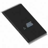
AT49BV320D-70TU Atmel, AT49BV320D-70TU Datasheet

AT49BV320D-70TU
Specifications of AT49BV320D-70TU
Available stocks
Related parts for AT49BV320D-70TU
AT49BV320D-70TU Summary of contents
Page 1
... Green (Pb/Halide-free) Packaging 1. Description The AT49BV320D( 2.7-volt 32-megabit Flash memory organized as 2,097,152 words of 16 bits each. The memory is divided into 71 sectors for erase operations. The device is offered in a 48-lead TSOP package and a 47-ball CBGA package. The device has CE and OE control signals to avoid any bus contention. This device can be read or reprogrammed using a single power supply, making it ideally suited for in-sys- tem programming ...
Page 2
... and D , must only differ in address A0. This command should be used during IN0 IN1 16. *NOTICE: + 0.6V CC AT49BV320D(T) 2nd Bus 3rd Bus Cycle Cycle Addr Data Addr ( Addr D IN Addr0 D Addr1 IN0 ( ( ( ( OUT (5) Addr FFFD ( OUT = 9.5V. The addresses, PP “Protection Regis- Stresses beyond those listed under “Absolute Maximum Ratings” ...
Page 3
... Standby/Program Inhibit V Program Inhibit Output Disable Reset Product Identification Software Notes: 1. The VPP pin can be tied can Refer to AC programming waveforms (min) = 1.65V. IHPP 5. V (max) = 0.4V. ILPP 6. Manufacturer Code: 001FH, Device Code: 90C5H – AT49BV320D; 90C4H – AT49BV320DT Ind RESET (2) X ...
Page 4
... Active Read Current Programming Current CC1 Input Load Current PP1 PP V Input Low Voltage IL V Input High Voltage IH V Output Low Voltage OL V Output High Voltage OH Note the erase mode mA. CC AT49BV320D(T) 22 Condition Min I 0. MHz OUT V - 0.6 CCQ -100 µ 0.1 ...
Page 5
... Input Test Waveforms and Measurement Level 30. Output Test Load 31. Pin Capacitance ( MHz 25°C Symbol Typ OUT Note: This parameter is characterized and is not 100% tested. 2.0V 1.5V 0. < CCQ 1.8 30 1.3 Max Units AT49BV320D(T) Conditions OUT 23 ...
Page 6
... OE or CE, whichever occurs first ( pF This parameter is characterized and is not 100% tested. AT49BV320D(T) 24 (1)(2)(3)( ADDRESS VALID ACC t RO HIGH Z OUTPUT VALID - t after the address transition without impact after the falling edge of CE without impact AT49BV320D(T)-70 Min Max Units 100 ACC after an address change ...
Page 7
... Address Hold Time AH t Chip Select Setup Time CS t Chip Select Hold Time CH t Write Pulse Width ( Write Pulse Width High WPH t Data Setup Time Data, OE Hold Time DH OEH 35. AC Word Load Waveforms 35.1 WE Controlled 35.2 CE Controlled AT49BV320D(T) Min Max Units ...
Page 8
... A20 DATA 38. Sector Erase Cycle Waveforms ( A0-A20 DATA Notes: 1. Any address can be used to load the data must be high only when WE and CE are both low. 3. The data can be 40H or 10H. 4. The address depends on what sector erased. AT49BV320D(T) 26 Min 500 PROGRAM CYCLE WPH ...
Page 9
... Active Standby 70 25 0.025 47C1 47-ball, Plastic Chip-Size Ball Grid Array Package (CBGA) 48T 48-lead, Plastic Thin Small Outline Package (TSOP) Ordering Code AT49BV320D-70CU AT49BV320D-70TU AT49BV320DT-70CU AT49BV320DT-70TU Package Type AT49BV320D(T) Package Operation Range 47C1 48T Industrial (-40° to 85° C) 47C1 ...
Page 10
... E is 0.15 mm per side and 0.25 mm per side. 3. Lead coplanarity is 0.10 mm maximum. 2325 Orchard Parkway San Jose, CA 95131 R PIN SEATING PLANE A1 TITLE 48T, 48-lead ( Package) Plastic Thin Small Outline Package, Type I (TSOP) AT49BV320D(T) 0º ~ 8º GAGE PLANE COMMON DIMENSIONS (Unit of Measure = mm) MIN NOM MAX SYMBOL A – – ...


