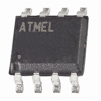
AT45DB041D-SSU-2.5 Atmel, AT45DB041D-SSU-2.5 Datasheet - Page 38

AT45DB041D-SSU-2.5
Manufacturer Part Number
AT45DB041D-SSU-2.5
Description
IC FLASH 4MBIT 66MHZ 8SOIC
Manufacturer
Atmel
Datasheet
1.AT45DB041D-MU.pdf
(55 pages)
Specifications of AT45DB041D-SSU-2.5
Format - Memory
FLASH
Memory Type
DataFLASH
Memory Size
4M (2048 pages x 264 bytes)
Speed
66MHz
Interface
SPI, RapidS
Voltage - Supply
2.5 V ~ 3.6 V
Operating Temperature
-40°C ~ 85°C
Package / Case
8-SOIC (3.9mm Width)
Architecture
Sectored
Interface Type
SPI
Supply Voltage (max)
3.6 V
Supply Voltage (min)
2.5 V
Maximum Operating Current
15 mA
Mounting Style
SMD/SMT
Organization
64 KB x 8
Lead Free Status / RoHS Status
Lead free / RoHS Compliant
Available stocks
Company
Part Number
Manufacturer
Quantity
Price
Part Number:
AT45DB041D-SSU-2.5
Manufacturer:
ATMEL/爱特梅尔
Quantity:
20 000
21.5
Figure 21-1. RapidS Mode
38
MOSI = Master Out, Slave In
MISO = Master In, Slave Out
The Master is the host controller and the Slave is the DataFlash
The Master always clocks data out on the rising edge of SCK and always clocks data in on the falling edge of SCK.
The Slave always clocks data out on the falling edge of SCK and always clocks data in on the rising edge of SCK.
Slave
Utilizing the RapidS Function
A.
B.
C.
D.
E.
F.
G. Master clocks in first bit of BYTE-SO.
H. Slave clocks out second bit of BYTE-SO.
I.
MOSI
MISO
AT45DB041D
SCK
Master clocks out first bit of BYTE-MOSI on the rising edge of SCK.
Slave clocks in first bit of BYTE-MOSI on the next rising edge of SCK.
Master clocks out second bit of BYTE-MOSI on the same rising edge of SCK.
Last bit of BYTE-MOSI is clocked out from the Master.
Last bit of BYTE-MOSI is clocked into the slave.
Slave clocks out first bit of BYTE-SO.
Master clocks in last bit of BYTE-SO.
CS
A
To take advantage of the RapidS function's ability to operate at higher clock frequencies, a full
clock cycle must be used to transmit data back and forth across the serial bus. The DataFlash is
designed to always clock its data out on the falling edge of the SCK signal and clock data in on
the rising edge of SCK.
For full clock cycle operation to be achieved, when the DataFlash is clocking data out on the
falling edge of SCK, the host controller should wait until the next falling edge of SCK to latch the
data in. Similarly, the host controller should clock its data out on the rising edge of SCK in
order to give the DataFlash a full clock cycle to latch the incoming data in on the next rising edge
of SCK.
1
B
MSB
C
2
3
4
BYTE-MOSI
5
6
7
D
8
E
LSB
F
1
G
MSB
2
H
3
4
BYTE-SO
5
6
7
8
3595P–DFLASH–09/09
I
LSB
1


