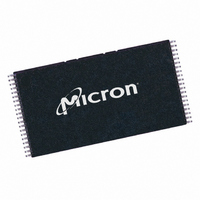
MT28F008B3VG-9 B Micron Technology Inc, MT28F008B3VG-9 B Datasheet - Page 4

MT28F008B3VG-9 B
Manufacturer Part Number
MT28F008B3VG-9 B
Description
IC FLASH 8MBIT 90NS 40TSOP
Manufacturer
Micron Technology Inc
Datasheet
1.MT28F008B3VG-9_B.pdf
(30 pages)
Specifications of MT28F008B3VG-9 B
Format - Memory
FLASH
Memory Type
FLASH - Nor
Memory Size
8M (1M x 8)
Speed
90ns
Interface
Parallel
Voltage - Supply
3 V ~ 3.6 V
Operating Temperature
0°C ~ 70°C
Package / Case
40-TSOP
Lead Free Status / RoHS Status
Contains lead / RoHS non-compliant
Table 1:
09005aef81136a91
Q10.fm - Rev. E 6/04 EN
11, 10, 9, 8,
NUMBERS
42, 41, 40,
39, 38, 37,
36, 35, 34,
15, 17, 19,
21, 24, 26,
16, 18, 20,
22, 25, 27,
7, 6, 5, 4,
44-PIN
28, 30
13, 32
SOP
3, 2
43
12
44
14
33
31
29
23
1
–
–
15, 14, 8, 7,
NUMBERS
21, 20, 19,
18, 17, 16,
36, 6, 5, 4,
3, 2, 1, 40,
25, 26, 27,
28, 32, 33,
Pin Descriptions
40-PIN
13, 37
34, 35
30, 31
23, 39
TSOP
29,38
12
22
10
24
11
9
–
–
–
1, 48, 17, 16
19, 18, 8, 7,
6, 5, 4, 3, 2,
NUMBERS
25, 24, 23,
22, 21, 20,
29, 31, 33,
35, 38, 40,
30, 32, 34,
36, 39, 41,
9,10,15
48-PIN
27, 46
42, 44
TSOP
11
14
47
45
43
13
37
26
12
28
SYMBOL
A0–A18/
BYTE#
DQ15/
DQ0–
DQ8–
DQ14
(A19)
(A-1)
WE#
WP#
DQ7
OE#
CE#
RP#
Vcc
V
V
NC
PP
SS
SMART 3 BOOT BLOCK FLASH MEMORY
Output
Output
Output
Supply
Supply
Supply
Input/
Input/
Input/
TYPE
Input
Input
Input
Input
Input
Input
Input
–
4
Write Enable: Determines if a given cycle is a WRITE cycle.
If WE# is LOW, the cycle is either a WRITE to the command
execution logic (CEL) or to the memory array.
Write Protect: Unlocks the boot block when HIGH if V
V
ERASE. Does not affect WRITE or ERASE operation on
other blocks.
Chip Enable: Activates the device when LOW. When CE# is
HIGH, the device is disabled and goes into standby power
mode.
Reset/Power-Down: When LOW, RP# clears the status
register, sets the internal state machine (ISM) to the array
read mode and places the device in deep power-down
mode. All inputs, including CE#, are “Don’t Care,” and all
outputs are High-Z. RP# unlocks the boot block and
overrides the condition of WP# when at V
must be held at V
Output Enable: Enables data output buffers when LOW.
When OE# is HIGH, the output buffers are disabled.
Byte Enable: If BYTE# = HIGH, the upper byte is active
through DQ8–DQ15. If BYTE# = LOW, DQ8–DQ14 are High-
Z, and all data is accessed through DQ0–DQ7. DQ15/(A-1)
becomes the least significant address input.
Address Inputs: Select a unique 16-bit word or 8-bit byte.
The DQ15/(A-1) input becomes the lowest order address
when BYTE# = LOW (MT28F800B3) to allow for a selection
of an 8-bit byte from the 1,048,576 available.
Data I/O: MSB of data when BYTE# = HIGH. Address Input:
LSB of address input when BYTE# = LOW during READ or
WRITE operation.
Data I/Os: Data output pins during any READ operation or
data input pins during a WRITE. These pins are used to
input commands to the CEL.
Data I/Os: Data output pins during any READ operation or
data input pins during a WRITE when BYTE# = HIGH. These
pins are High-Z when BYTE# is LOW.
Write/Erase Supply Voltage: From a WRITE or ERASE
CONFIRM until completion of the WRITE or ERASE, V
must be at V
during all other operations.
Power Supply: +3.3V ±0.3V.
Ground.
NoConnect:Thesepinsmaybedrivenorleftunconnected.
PPH
1 (3.3V) or V
Micron Technology, Inc., reserves the right to change products or specifications without notice.
PPH
1 (3.3V) or V
PPH
IH
2 (5V) and RP# = V
during all other modes of operation.
DESCRIPTION
PPH
2 (5V). V
©2001 Micron Technology, Inc. All rights reserved.
IH
PP
during a WRITE or
HH
= “Don’t Care”
(12V), and
8Mb
PP
PP
=


