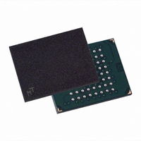
MT28F128J3FS-12 MET Micron Technology Inc, MT28F128J3FS-12 MET Datasheet - Page 16

MT28F128J3FS-12 MET
Manufacturer Part Number
MT28F128J3FS-12 MET
Description
IC FLASH 128MBIT 120NS 64FBGA
Manufacturer
Micron Technology Inc
Datasheet
1.MT28F128J3FS-12_ET_TR.pdf
(55 pages)
Specifications of MT28F128J3FS-12 MET
Format - Memory
FLASH
Memory Type
FLASH
Memory Size
128M (16Mx8, 8Mx16)
Speed
120ns
Interface
Parallel
Voltage - Supply
2.7 V ~ 3.6 V
Operating Temperature
-40°C ~ 85°C
Package / Case
64-FBGA
Lead Free Status / RoHS Status
Contains lead / RoHS non-compliant
READ ARRAY Command
device power-up and after exiting reset/power-down
mode. The read configuration register defaults to
asynchronous read page mode. Until another com-
mand is written, the READ ARRAY command also
causes the device to enter read array mode. When the
ISM has started a block erase, program, or lock bit con-
figuration, the device does not recognize the READ
ARRAY command until the ISM completes its opera-
tion, unless the ISM is suspended via an ERASE or
PROGRAM SUSPEND command. The READ ARRAY
command functions independently of the V
age.
READ QUERY MODE Command
structure or “data base” returned by the CFI QUERY
command. System software should retain this struc-
ture to gain critical information such as block size,
density, x8/x16, and electrical specifications. When
this information has been obtained, the software
knows which command sets to use to enable Flash
writes or block erases, and otherwise control the Flash
component.
Table 5:
NOTE:
09005aef80b5a323
MT28F640J3.fm – Rev. N 3/05 EN
DEVICE
TYPE/MODE
x16 device
x16 mode
x16 device
x8 mode
1. The system must drive the lowest-order addresses to access all the device’s array data when the device is configured
The device defaults to read array mode upon initial
This section is related to the definition of the data
in x8 mode. Therefore, word addressing where these lower addresses are not toggled by the system is “Not Applica-
ble” for x8-configured devices.
Summary of Query-Structure Output as a Function of Device and Mode
MAXIMUM DEVICE BUS WIDTH
QUERY START LOCATION IN
ADDRESSES
N/A
10h
1
PEN
QUERY DATA WITH MAXIMUM
OFFSET
volt-
HEX
10
11
12
DEVICE BUS WIDTH
16
ADDRESSING
Query Structure Output
obtain information about controlling the Flash com-
ponent. The device’s CFI-compliant interface allows
the host system to access query data. Query data are
always located on the lowest-order data outputs
(DQ0–DQ7) only. The numerical offset value is the
address relative to the maximum bus width supported
by the device. On this family of devices, the query table
device starting address is a 10h, which is a word
address for x16 devices.
query structure, “Q” and “R” in ASCII, appear on the
low byte at word addresses 10h and 11h. This CFI-
compliant device outputs 00h data on upper bytes,
thus making the device output ASCII “Q” on the LOW
byte (DQ7–DQ0) and 00h on the HIGH byte (DQ15–
DQ8). At query addresses containing two or more
bytes of information, the least significant data byte is
located at the lower address, and the most significant
data byte is located at the higher address. This is sum-
marized in Table 5. A more detailed example is pro-
vided in Table 6.
CODE
0051
0052
0059
N/A
The query “data base” enables system software to
For a x16 organization, the first two bytes of the
HEX
Micron Technology, Inc., reserves the right to change products or specifications without notice.
1
VALUE
ASCII
Q
Y
R
128Mb, 64Mb, 32Mb
Q-FLASH MEMORY
OFFSET
HEX
QUERY DATA WITH BYTE
20
21
22
20
21
22
ADDRESSING
CODE
HEX
51
00
52
51
51
52
©2000 Micron Technology. Inc.
VALUE
ASCII
Null
Q
Q
Q
R
R


