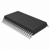
MT28F800B5SG-8 BET TR Micron Technology Inc, MT28F800B5SG-8 BET TR Datasheet - Page 8

MT28F800B5SG-8 BET TR
Manufacturer Part Number
MT28F800B5SG-8 BET TR
Description
IC FLASH 8MBIT 80NS 44SOP
Manufacturer
Micron Technology Inc
Datasheet
1.MT28F008B5VG-8_B.pdf
(30 pages)
Specifications of MT28F800B5SG-8 BET TR
Format - Memory
FLASH
Memory Type
FLASH - Nor
Memory Size
8M (1M x 8 or 512K x 16)
Speed
80ns
Interface
Parallel
Voltage - Supply
4.5 V ~ 5.5 V
Operating Temperature
-40°C ~ 85°C
Package / Case
44-SOP
Lead Free Status / RoHS Status
Contains lead / RoHS non-compliant
tional error information is set in three other bits: V
status, write status, and erase status.
Command Execution Cell (CEL)
device. These commands control the operation of the
ISM and the read path (i.e., memory array, ID register
or status register). Commands may be issued to the
CEL while the ISM is active. However, there are restric-
tions on what commands are allowed in this condition.
See the Command Execution section for more detail.
Deep Power-Down Mode
MT28F800B5 and MT28F008B5 feature a very low cur-
rent, deep power-down mode. To enter this mode, the
RP# pin is taken to V
draw is a maximum of 20µA. Entering deep power-
down also clears the status register and sets the ISM to
the read array mode.
MEMORY ARCHITECTURE
architecture is designed to allow sections to be erased
without disturbing the rest of the array. The array is
divided into eleven addressable blocks that vary in size
and are independently erasable. When blocks rather
than the entire array are erased, total device endur-
ance is enhanced, as is system flexibility. Only the
09005aef8075d1ec
MT28F800B5_4.fm - Rev. 4, Pub. 2/2004
The CEL receives and interprets commands to the
To allow for maximum power conservation, the
The MT28F800B5 and MT28F008B5 memory array
MT28F800B5/008B5xx-xxB
WORD ADDRESS
70000h
60000h
50000h
40000h
30000h
20000h
10000h
04000h
03000h
02000h
00000h
7FFFFh
6FFFFh
5FFFFh
4FFFFh
3FFFFh
2FFFFh
1FFFFh
0FFFFh
03FFFh
02FFFh
01FFFh
Bottom Boot
SS
BYTE ADDRESS
±0.2V. In this mode, the current
A0000h
E0000h
C0000h
80000h
60000h
40000h
20000h
08000h
06000h
04000h
00000h
DFFFFh
BFFFFh
07FFFh
05FFFh
03FFFh
FFFFFh
9FFFFh
7FFFFh
5FFFFh
3FFFFh
1FFFFh
8KB Parameter Block
8KB Parameter Block
128KB Main Block
128KB Main Block
128KB Main Block
128KB Main Block
128KB Main Block
128KB Main Block
128KB Main Block
96KB Main Block
16KB Boot Block
Figure 1: Memory Address Maps
SMART 5 BOOT BLOCK FLASH MEMORY
PP
8
ERASE function is block-oriented. All READ and
WRITE operations are done on a random-access basis.
ERASE or WRITE with a hardware protection circuit
which requires that a super-voltage be applied to RP#
or that the WP# pin be driven HIGH before erasure is
commenced. The boot block is intended for the core
firmware required for basic system functionality. The
remaining ten blocks do not require that either of
these two conditions be met before WRITE or ERASE
operations.
Boot Block
security for the most sensitive portions of the firm-
ware. This 16KB block may only be erased or written
when the RP# pin is at the specified boot block unlock
voltage (V
WRITE or ERASE of the boot block, the RP# pin must
be held at V
WRITE or ERASE is completed. (The WP# pin does not
apply to the SOP package.) The V
V
two configurations and top or bottom boot block. The
top boot block version supports processors of the x86
variety. The bottom boot block version is intended for
680X0 and RISC applications. Figure 1 illustrates the
memory address maps associated with these two ver-
sions.
PPH
The boot block is protected from unintentional
The hardware-protected boot block provides extra
The MT28F800B5 and MT28F008B5 are available in
(5V) when the boot block is written to or erased.
Micron Technology, Inc., reserves the right to change products or specifications without notice.
MT28F800B5/008B5xx-xxT
HH
WORD ADDRESS
HH
) or when the WP# pin is HIGH. During a
7D000h
7E000h
7DFFFh
7C000h
70000h
60000h
50000h
40000h
30000h
20000h
10000h
00000h
7CFFFh
7BFFFh
7FFFFh
6FFFFh
5FFFFh
4FFFFh
3FFFFh
2FFFFh
1FFFFh
0FFFFh
or the WP# pin held HIGH until the
Top Boot
BYTE ADDRESS
A0000h
FA000h
C0000h
FC000h
F8000h
E0000h
DFFFFh
80000h
60000h
40000h
20000h
00000h
FBFFFh
F9FFFh
F7FFFh
BFFFFh
9FFFFh
7FFFFh
5FFFFh
3FFFFh
1FFFFh
FFFFFh
8KB Parameter Block
8KB Parameter Block
128KB Main Block
128KB Main Block
128KB Main Block
128KB Main Block
128KB Main Block
128KB Main Block
128KB Main Block
96KB Main Block
16KB Boot Block
PP
pin must be at
©2002 Micron Technology Inc.
8Mb


