CY7C199-12VC Cypress Semiconductor Corp, CY7C199-12VC Datasheet
CY7C199-12VC
Specifications of CY7C199-12VC
Available stocks


Related parts for CY7C199-12VC


CY7C199-12VC Summary of contents
Page 1
... LOW Chip Enable (CE) and active LOW Output Enable (OE) and three-state drivers. This device has an automatic power-down feature, reducing the power con- sumption by 81% when deselected. The CY7C199 is in the standard 300-mil-wide DIP, SOJ, and LCC packages. An active LOW Write Enable signal (WE) controls the writ- ing/reading operation of the memory ...
Page 2
... L = 1/t RC Mil , Com’ MAX , Com’l 0.5 CC – 0. 0.05 – 0.3V CC Mil < 0.3V CY7C199 [1] ................................... –0. [1] ................................ –0. 7C199-10 7C199-12 7C199-15 Min. Max. Min. Max. Min. 2.4 2.4 2.4 0.4 0.4 2.2 V 2 +0.3V +0.3V –0.5 0.8 –0.5 0.8 – ...
Page 3
... Min. Max. Min. 2.4 2.4 2.4 0.4 0.4 2.2 V 2 +0.3V +0.3V -0.5 0.8 -0.5 0.8 -0.5 –5 +5 –5 +5 –5 –5 +5 –5 +5 –5 150 140 80 70 150 150 0.05 0. Max CY7C199 Max. Unit V 0 +0.3V 0 140 150 0. Unit pF pF Page ...
Page 4
... Over the Operating Range (L version only) Conditions Com’ 2.0V > V – 0.3V, CC Com’ > V – 0. < 0.3V IN DATA RETENTION MODE 3.0V V > CDR CY7C199 ALL INPUT PULSES 3.0V 90% 90% 10% GND t r [6] Min. Max. 2 200 3. 10 C199–6 Unit C199– ...
Page 5
... less than less than t HZCE LZCE HZOE LZOE = part ( Test Loads. Transition is measured 500 mV from steady-state voltage. HZWE 7C199-12 7C199-15 Max. Min. Max. Min and t is less than t for any given device. HZWE LZWE and CY7C199 Max. Unit Page ...
Page 6
... Read Cycle No. 1 ADDRESS DATA OUT PREVIOUS DATA VALID Notes: 12. Device is continuously selected HIGH for read cycle. Document #: 38-05160 Rev. ** [3,7] (continued) 7C199-20 7C199-25 Min. Max. Min [ [ [ OHA . IL CY7C199 7C199-35 7C199-45 Max. Min. Max. Min. Max DATA VALID Unit ...
Page 7
... If CE goes HIGH simultaneously with WE HIGH, the output remains in a high-impedance state. Document #: 38-05160 Rev ACE t DOE t LZOE 50 PWE t SD DATA SCE DATA t HZOE t HZCE DATA VALID VALID VALID IN CY7C199 HIGH IMPEDANCE ICC ISB C199–9 C199–10 C199–11 Page ...
Page 8
... IN t LZWE OUTPUT SOURCE CURRENT vs. OUTPUT VOLTAGE 120 100 125 0.0 1.0 2.0 OUTPUT VOLTAGE (V) OUTPUT SINK CURRENT vs. OUTPUT VOLTAGE 140 120 100 0.0 1.0 2.0 125 OUTPUT VOLTAGE (V) CY7C199 C199–12 =5.0V =25 C 3.0 4.0 =5.0V =25 C 3.0 4.0 Page ...
Page 9
... CY7C199L-8VC CY7C199L-8ZC 10 CY7C199-10VC CY7C199-10ZC CY7C199L-10VC CY7C199L-10ZC CY7C199-10VI CY7C199-10ZI CY7C199L-10VI CY7C199L-10ZI 12 CY7C199-12PC CY7C199-12VC CY7C199-12ZC CY7C199L-12PC CY7C199L-12VC CY7C199L-12ZC CY7C199-12VI CY7C199-12ZI CY7C199L-12VI CY7C199L-12ZI Shaded area contains advance information. Contact your Cypress sales representative for availability Document #: 38-05160 Rev. ** (continued) TYPICAL ACCESS TIME CHANGE vs. OUTPUT LOADING 30 ...
Page 10
... CY7C199-20PC CY7C199-20VC CY7C199-20ZC CY7C199L-20PC CY7C199L-20VC CY7C199L-20ZC CY7C199-20VI CY7C199-20ZI CY7C199-20DMB CY7C199-20LMB CY7C199L-20DMB CY7C199L-20LMB 25 CY7C199-25PC CY7C199-25SC CY7C199-25VC CY7C199-25ZC CY7C199L-25ZI CY7C199-25DMB CY7C199-25LMB 35 CY7C199-35PC CY7C199-35SC CY7C199-35VC CY7C199-35ZC CY7C199-35DMB CY7C199-35LMB 45 CY7C199-45DMB CY7C199-45LMB Shaded area contains advance information. Contact your Cypress sales representative for availability Document #: 38-05160 Rev. ** ...
Page 11
... MILITARY SPECIFICATIONS Group A Subgroup Testing DC Characteristics Parameter Max SB1 I SB2 Switching Characteristics Parameter READ CYCLE OHA t ACE t DOE WRITE CYCLE PWE Document #: 38-05160 Rev. ** Subgroups Subgroups 10, 11 CY7C199 Page ...
Page 12
... Package Diagrams Document #: 38-05160 Rev. ** 28-Lead (300-Mil) CerDIP D22 MIL-STD-1835 D-15 Config. A CY7C199 51-80032 Page ...
Page 13
... Package Diagrams (continued) Document #: 38-05160 Rev. ** 28-Pin Rectangular Leadless Chip Carrier L54 MIL-STD-1835 C-11A 28-Lead (300-Mil) Molded DIP P21 CY7C199 51-80067 51-85014-B Page ...
Page 14
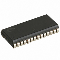
... Package Diagrams (continued) Document #: 38-05160 Rev. ** 28-Lead (300-Mil) Molded SOIC S21 28-Lead (300-Mil) Molded SOJ V21 CY7C199 51-85026-A 51-85031-B Page ...
Page 15
... Cypress Semiconductor product. Nor does it convey or imply any license under patent or other rights. Cypress Semiconductor does not authorize its products for use as critical components in life-support systems where a malfunction or failure may reasonably be expected to result in significant injury to the user. The inclusion of Cypress 28-Lead Thin Small Outline Package Z28 CY7C199 51-85071-F Page ...
Page 16
... Document Title: CY7C199 32K x 8 Static RAM Document Number: 38-05160 Issue REV. ECN NO. Date ** 109971 10/28/01 Document #: 38-05160 Rev. ** Orig. of Change Description of Change SZV Change from Spec number: 38-00239 to 38-05160 CY7C199 Page ...