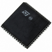
DSM2180F3V-15K6 STMicroelectronics, DSM2180F3V-15K6 Datasheet - Page 4

DSM2180F3V-15K6
Manufacturer Part Number
DSM2180F3V-15K6
Description
IC FLASH 1MBIT 150NS 52PLCC
Manufacturer
STMicroelectronics
Specifications of DSM2180F3V-15K6
Format - Memory
FLASH
Memory Type
FLASH
Memory Size
1M (128K x 8)
Speed
150ns
Interface
Parallel
Voltage - Supply
3 V ~ 3.6 V
Operating Temperature
-40°C ~ 85°C
Package / Case
52-PLCC
Operating Supply Voltage (typ)
3.3V
Operating Supply Voltage (min)
2.97V
Operating Supply Voltage (max)
3.63V
Mounting
Surface Mount
Pin Count
52
Lead Free Status / RoHS Status
Lead free / RoHS Compliant
Other names
497-1336-5
Available stocks
Company
Part Number
Manufacturer
Quantity
Price
Company:
Part Number:
DSM2180F3V-15K6
Manufacturer:
FREESCALE
Quantity:
101
Company:
Part Number:
DSM2180F3V-15K6
Manufacturer:
STMicroelectronics
Quantity:
10 000
DSM2180F3V
SUMMARY DESCRIPTION
These are system memory devices for use with
Digital Signal Processors from the popular Analog
Devices ADSP-218X family. DSM means Digital
signal processor System Memory. A DSM device
brings in-system programmable Flash memory,
programmable logic, and additional I/O to DSP
systems. The result is a simple and flexible two-
chip solution for DSP designs. DSM devices pro-
vide the flexibility of Flash memory and smart
JTAG programming techniques for both manufac-
turing and the field. On-chip integrated memory
decode logic and memory paging logic make it
easy to add large amounts of external Flash mem-
ory to the ADSP-218X family for bootloading upon
power-up and/or overlay memory. The DSP ac-
cesses this Flash memory using either its Byte
DMA (BDMA) interface or as external data overlay
memory (no DMA setup overhead).
Figure 2. PLCC Connections
JTAG In-System Programming (ISP) reduces de-
velopment time, simplifies manufacturing flow,
and lowers the cost of field upgrades. The JTAG
ISP interface eliminates the need for sockets and
pre-programmed memory and logic devices. For
manufacturing, end products may be assembled
with a blank DSM device soldered to the circuit
board and programmed at the end of the manufac-
turing line in 10 to 20 seconds with no involvement
of the DSP. This allows efficient means to test
4/63
GND
V CC
PD2
PD1
PD0
PC7
PC6
PC5
PC4
PC3
PC2
PC0
PC1
8
9
10
11
12
13
14
15
16
17
18
19
20
46
45
44
43
42
41
40
39
38
37
36
35
34
AD7
AD15
AD14
AD13
AD12
AD11
AD10
AD9
AD8
V CC
AD6
AD5
AD4
AI02857
product and manage inventory by rapidly pro-
gramming test code, then application code as de-
termined by inventory requirements (Just-In Time
inventory). Additionally, JTAG ISP reduces devel-
opment time by turning fast iterations of DSP code
in the lab. Code updates in the field require no dis-
assembly of product. The FlashLINK
gramming cable costs $59 USD and plugs into any
PC or note-book parallel port.
Figure 3. PQFP Connections
In addition to ISP Flash memory, DSM devices
add programmable logic (PLD) and up to 16 con-
figurable I/O pins to the DSP system. The state of
each I/O pin can be driven by DSP software or
PLD logic. PLD and I/O configuration are program-
mable by JTAG ISP, just like the Flash memory.
The PLD consists of more than 3000 gates and
has 16 macro cell registers. Common uses for the
PLD include chip selects for external devices (i.e.
UART), state-machines, simple shifters and coun-
ters, keypad and control panel interfaces, clock di-
viders, handshake delay, muxes, etc. This
eliminates the need for small external PLDs and
logic devices. Configuration of PLD, I/O, and Flash
memory mapping are easily entered in a point-
and-click environment using the software develop-
ment tool, PSDsoft Express
available at no charge from www.psdst.com.
PD2
PD1
PD0
PC7
PC6
PC5
PC4
V
GND
PC3
PC2
PC1
PC0
CC
1
2
3
4
5
6
7
8
9
10
11
12
13
TM
. This software is
TM
JTAG pro-
39 AD15
38 AD14
37 AD13
36 AD12
35 AD11
34 AD10
33 AD9
32 AD8
31 V
30 AD7
29 AD6
28 AD5
27 AD4
CC
AI02858


