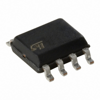
M93C66-WMN6 STMicroelectronics, M93C66-WMN6 Datasheet - Page 27

M93C66-WMN6
Manufacturer Part Number
M93C66-WMN6
Description
IC EEPROM 4KBIT 2MHZ 8SOIC
Manufacturer
STMicroelectronics
Datasheet
1.M93C46-WMN6TP.pdf
(36 pages)
Specifications of M93C66-WMN6
Format - Memory
EEPROMs - Serial
Memory Type
EEPROM
Memory Size
4K (512 x 8 or 256 x 16)
Speed
2MHz
Interface
Microwire, 3-Wire Serial
Voltage - Supply
2.5 V ~ 5.5 V
Operating Temperature
-40°C ~ 85°C
Package / Case
8-SOIC (3.9mm Width)
Lead Free Status / RoHS Status
Contains lead / RoHS non-compliant
Other names
497-1934-5
Available stocks
Company
Part Number
Manufacturer
Quantity
Price
Part Number:
M93C66-WMN6P
Manufacturer:
ST
Quantity:
20 000
Company:
Part Number:
M93C66-WMN6T
Manufacturer:
ST
Quantity:
881
Part Number:
M93C66-WMN6T
Manufacturer:
ST
Quantity:
20 000
Company:
Part Number:
M93C66-WMN6TP
Manufacturer:
ST
Quantity:
50 000
Part Number:
M93C66-WMN6TP
Manufacturer:
ST
Quantity:
20 000
M93C86, M93C76, M93C66, M93C56, M93C46
Table 23.
1. This product is under development. For more information, please contact your nearest ST sales office.
2. Chip Select Input (S) must be brought low for a minimum of t
3. t
Figure 9.
Symbol
t
t
t
CHCL
CLCH
SLSH
t
t
t
t
t
t
t
t
t
t
CHQV
SHCH
DVCH
CHDX
SHQV
CHQL
SLCH
CLSH
SLQZ
CLSL
CHCL
t
f
W
C
(2)
(3)
(3)
C
S
D
+ t
CLCH
t
t
t
t
t
t
t
t
AC characteristics (M93Cx6-R)
Alt.
t
t
Synchronous timing (start and op-code input)
t
CSH
f
CSS
SKH
SKS
t
t
SKL
PD0
PD1
DIS
DIH
WP
CS
SK
SV
DF
1 / f
C
Clock frequency
Chip Select low to Clock high
Chip Select setup time
Chip Select low to Chip Select high
Clock high time
Clock low time
Data in setup time
Data in hold time
Clock setup time (relative to S)
Chip Select hold time
Chip Select to READY/BUSY status
Chip Select low to output Hi-Z
Delay to output low
Delay to output valid
Erase or Write cycle time
.
Test conditions specified in
Doc ID 4997 Rev 11
tCLSH
START
START
Parameter
tSHCH
tDVCH
OP CODE
Table 13.
SLSH
OP CODE INPUT
between consecutive instruction cycles.
and
tCHCL
Table 11.
OP CODE
Min.
D.C.
250
250
250
100
100
100
250
50
0
DC and AC parameters
tCLCH
(1)
Max.
400
200
400
400
AI01428
10
tCHDX
1
(1)
MHz
Unit
ms
ns
ns
ns
ns
ns
ns
ns
ns
ns
ns
ns
ns
ns
27/36


