CY7C1009B-15VXC Cypress Semiconductor Corp, CY7C1009B-15VXC Datasheet
CY7C1009B-15VXC
Specifications of CY7C1009B-15VXC
Available stocks


Related parts for CY7C1009B-15VXC


CY7C1009B-15VXC Summary of contents
Page 1
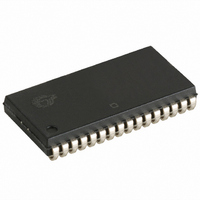
... HIGH or CE LOW), the outputs are disabled (OE HIGH during a write operation (CE CY7C109B is available in standard 400-mil-wide SOJ and 32- pin TSOP type I packages. The CY7C1009B is available in a 300-mil-wide SOJ package. The CY7C109B and CY7C1009B are functionally equivalent in all other respects I/O 0 I/O ...
Page 2
... IN IL MAX , CC > V – 0.3V < 0.3V, 2 > V – 0.3V < 0.3V Test Conditions T = 25° MHz 5.0V CC CY7C109B CY7C1009B 7C109B-15 7C109B-20 7C1009B-15 7C1009B- Ambient Temperature 0°C to +70°C −40°C to +85°C 7C109B-15 7C109B-20 7C1009B-15 7C1009B-20 Max. Min. Max. Min. 2.4 2.4 ...
Page 3
... LOW to High Z 2 HIGH to Power- LOW to Power-Down 2 12 HIGH to Write End less than less than t HZCE LZCE HZOE LOW, CE HIGH, and WE LOW CY7C109B CY7C1009B ALL INPUT PULSES 90% 10% ≤ THÉ VENIN EQUIVALENT 167Ω 1.73V 7C109B-15 7C109B-20 7C1009B-15 7C1009B-20 Max. Min. Max. Min ...
Page 4
... CC V > V – 0. DATA RETENTION MODE 4.5V V > CDR OHA ACE t DOE t LZOE 50 transition LOW and CE transition HIGH. 2 CY7C109B CY7C1009B Min. Max. + 0.5V 2.0 CC 150 < 0.3V < 0.3V IN 200 4. DATA VALID t HZOE t HZCE IMPEDANCE DATA VALID t PD 50% Unit V µA ns µs HIGH Page ...
Page 5
... LOW simultaneously with WE going HIGH, the output remains in a high-impedance state 15. During this period the I/Os are in the output state and input signals should not be applied. Document #: 38-05038 Rev. *C [13, 14 SCE SCE PWE t SD DATA VALID [13, 14 SCE t SCE PWE t SD DATA VALID IN CY7C109B CY7C1009B Page ...
Page 6
... DATA I/O Truth Table High High Data Out Data High Z Document #: 38-05038 Rev. *C [14 SCE t SCE PWE t HZWE I/O –I Power-Down Power-Down Read Write Selected, Outputs Disabled CY7C109B CY7C1009B DATA VALID t LZWE Mode Power Standby (I Standby (I Active (I CC Active (I CC Active ( Page ...
Page 7
... Ordering Information Speed (ns) Ordering Code 12 CY7C109B-12VC CY7C1009B-12VC CY7C109B-12ZC CY7C109B-12ZXC 15 CY7C109BL-15VC CY7C109B-15VC CY7C109B-15VXC CY7C1009B-15VC CY7C1009B-15VXC CY7C109B-15ZC CY7C109B-15ZXC CY7C109B-15VI CY7C1009B-15VI 20 CY7C109B-20ZC CY7C1009B-20VC CY7C109B-20VI Please contact local sales representative regarding availability of parts Package Diagrams Document #: 38-05038 Rev. *C Package Diagram Package Type 51-85033 32-pin (400-Mil) Molded SOJ ...
Page 8
... Package Diagrams (continued) Document #: 38-05038 Rev. *C 32-pin (400-Mil) Molded SOJ (51-85033) CY7C109B CY7C1009B 51-85033-*B Page ...
Page 9
... The inclusion of Cypress products in life-support systems application implies that the manufacturer assumes all risk of such use and in doing so indemnifies Cypress against all charges. CY7C109B CY7C1009B 51-85056-*D Page ...
Page 10
... Document History Page Document Title: CY7C109B/CY7C1009B 128K x 8 Static RAM Document Number: 38-05038 Issue REV. ECN NO. Date ** 106832 09/22/01 *A 116467 09/16/02 *B 397875 See ECN *C 493543 See ECN Document #: 38-05038 Rev. *C Orig. of Change Description of Change SZV Change from Spec number: 38-00971 to 38-05038 ...