CY7C1399B-15VXI Cypress Semiconductor Corp, CY7C1399B-15VXI Datasheet - Page 2
CY7C1399B-15VXI
Manufacturer Part Number
CY7C1399B-15VXI
Description
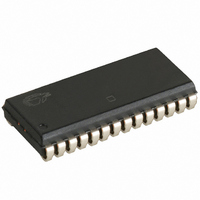
IC SRAM 256KBIT 15NS 28SOJ
Manufacturer
Cypress Semiconductor Corp
Datasheet
1.CY7C1399B-12VXC.pdf
(10 pages)
Specifications of CY7C1399B-15VXI
Format - Memory
RAM
Memory Type
SRAM - Asynchronous
Memory Size
256K (32K x 8)
Speed
15ns
Interface
Parallel
Voltage - Supply
3 V ~ 3.6 V
Operating Temperature
-40°C ~ 85°C
Package / Case
28-SOJ
Lead Free Status / RoHS Status
Lead free / RoHS Compliant


Document #: 38-05071 Rev. *D
Pin Configuration
Maximum Ratings
(Above which the useful life may be impaired. For user guide-
lines, not tested.)
Storage Temperature ................................. –65°C to +150°C
Ambient Temperature with
Power Applied............................................. –55°C to +125°C
Supply Voltage on V
DC Voltage Applied to Outputs
in High Z State
DC Input Voltage
Electrical Characteristics
V
V
V
V
I
I
I
I
I
I
Notes:
Parameter
IX
OZ
OS
CC
SB1
SB2
2. Minimum voltage is equal to – 2.0V for pulse durations of less than 20 ns.
3. Not more than one output should be shorted at one time. Duration of the short circuit should not exceed 30 seconds.
4. Device draws low standby current regardless of switching on the addresses.
OH
OL
IH
IL
Output HIGH Voltage
Output LOW Voltage
Output Leakage
Current
Output Short
Circuit Current
Supply Current
Current — TTL Inputs
Current — CMOS Inputs
Input HIGH Voltage
Input LOW Voltage
Input Load Current
V
Automatic CE Power-Down
Automatic CE Power-Down
CC
[2]
[2]
....................................–0.5V to V
Operating
.................................–0.5V to V
CC
V
WE
A
A
OE
Description
CC
A
A
A
A
A
A
A
A
A
10
11
to Relative GND
1
2
3
4
5
6
7
8
9
[3]
22
23
24
25
26
4
5
6
7
27
28
1
2
3
[2]
Over the Operating Range
[4]
[2]
.... –0.5V to +4.6V
GND ≤ V
Output Disabled
f = f
Max. V
V
Max. V
V
WE ≥V
f = f
V
V
V
V
IN
CC
CC
CC
CC
CC
MAX
MAX
≥ V
– 0.3V, or V
= Min., I
= Min., I
= Max., V
= Max., I
CC
CC
CC
CC
CC
IH
= 1/t
+ 0.5V
+ 0.5V
Test Conditions
I
, or V
, CE ≥ V
, CE ≥ V
≤ V
– 0.3V or WE ≤0.3V,
Top View
TSOP
RC
OH
OL
CC
OUT
OUT
IN
[1]
= 4.0 mA
,
= –2.0 mA
IN
≤ V
CC
IH
= 0 mA,
≤ 0.3V,
= GND
,
IL
Output Current into Outputs (LOW)............................. 20 mA
Static Discharge Voltage........................................... >2001V
(per MIL-STD-883, Method 3015)
Latch-Up Current .................................................... >200 mA
Operating Range
– 0.3V, V
Commercial
Industrial
,f = f
Range
MAX
IN
≥
L
L
Min.
–0.3
7C1399B-10
2.4
2.2
–1
–5
–40
Temperature
0
°
Ambient
C to +70
°
C to +85
21
20
19
18
17
16
15
14
13
12
11
10
+0.3V
9
8
Max.
–300
V
500
0.4
0.8
+1
+5
60
50
5
4
CC
A
CE
I/O
I/O
I/O
I/O
I/O
GND
I/O
I/O
I/O
A
A
A
0
14
13
12
°
7
6
5
4
3
2
1
0
C
°
C
Min.
–0.3
7C1399B-12
2.4
2.2
–1
–5
CY7C1399B
3.3V ±300 mV
3.3V ±300 mV
+0.3V
Max.
–300
V
500
0.4
0.8
+1
+5
55
50
Page 2 of 10
5
4
CC
V
CC
Unit
mA
mA
mA
mA
µA
µA
µA
µA
V
V
V
V
Related parts for CY7C1399B-15VXI
Image
Part Number
Description
Manufacturer
Datasheet
Request
R

Part Number:
Description:
IC SRAM 256KBIT 15NS 28SOJ
Manufacturer:
Cypress Semiconductor Corp
Datasheet:
Part Number:
Description:
IC SRAM 256KBIT 12NS 28SOJ
Manufacturer:
Cypress Semiconductor Corp
Datasheet:

Part Number:
Description:
IC SRAM 256KBIT 12NS 28TSOP
Manufacturer:
Cypress Semiconductor Corp
Datasheet:
Part Number:
Description:
IC SRAM 256KBIT 15NS 28SOJ
Manufacturer:
Cypress Semiconductor Corp
Datasheet:
Part Number:
Description:
IC SRAM 256KBIT 15NS 28TSOP
Manufacturer:
Cypress Semiconductor Corp
Datasheet:
Part Number:
Description:
IC SRAM 256KBIT 12NS 28TSOP
Manufacturer:
Cypress Semiconductor Corp
Datasheet:
Part Number:
Description:
IC SRAM 256KBIT 15NS 28TSOP
Manufacturer:
Cypress Semiconductor Corp
Datasheet:
Part Number:
Description:
IC SRAM 256KBIT 15NS 28SOJ
Manufacturer:
Cypress Semiconductor Corp
Datasheet:

Part Number:
Description:
Manufacturer:
Cypress Semiconductor Corp
Datasheet:
Part Number:
Description:
Manufacturer:
Cypress Semiconductor Corp
Datasheet:
Part Number:
Description:
Manufacturer:
Cypress Semiconductor Corp
Datasheet:
Part Number:
Description:
Manufacturer:
Cypress Semiconductor Corp
Datasheet:
Part Number:
Description:
SRAM Chip Async Single 3.3V 256K-Bit 32K x 8 15ns 28-Pin TSOP-I
Manufacturer:
Cypress Semiconductor Corp
Part Number:
Description:
IC SRAM 256KBIT 12NS 28SOJ
Manufacturer:
Cypress Semiconductor Corp
Datasheet:
Part Number:
Description:
IC SRAM 256KBIT 12NS 28SOJ
Manufacturer:
Cypress Semiconductor Corp
Datasheet: