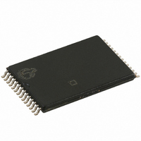
CY7C199C-15ZXCT Cypress Semiconductor Corp, CY7C199C-15ZXCT Datasheet - Page 6

CY7C199C-15ZXCT
Manufacturer Part Number
CY7C199C-15ZXCT
Description
IC SRAM 256KBIT 15NS 28TSOP
Manufacturer
Cypress Semiconductor Corp
Datasheet
1.CY7C199CL-15ZXC.pdf
(13 pages)
Specifications of CY7C199C-15ZXCT
Format - Memory
RAM
Memory Type
SRAM - Asynchronous
Memory Size
256K (32K x 8)
Speed
15ns
Interface
Parallel
Voltage - Supply
4.5 V ~ 5.5 V
Operating Temperature
0°C ~ 70°C
Package / Case
28-TSOP I
Lead Free Status / RoHS Status
Lead free / RoHS Compliant
Document #: 38-05408 Rev. *B
AC Electrical Characteristics
Data Retention Characteristics
Thermal Resistance
t
t
t
t
t
t
t
t
t
t
t
t
t
t
t
t
t
t
t
t
t
V
I
t
t
Notes:
RC
AA
OHA
ACE
DOE
LZOE
HZOE
LZCE
HZCE
PU
PD
WC
SCE
AW
HA
SA
PWE
SD
HD
HZWE
LZWE
CCDR
CDR
R
Parameter
Parameter
4. Test Conditions assume a transition time of 3 ns or less, timing reference levels of 1.5V, input pulse levels of 0 to 3.0V.
5. At any given temperature and voltage condition, t
6. The internal write time of the memory is defined by the overlap of CE LOW and WE LOW. CE and WE must be LOW to initiate a write, and the transition of any
7. t
8. L-version only.
Parameter
DR
of these signals can terminate the write. The input data set–up and hold timing should be referenced to the leading edge of the signal that terminates the write.
HZOE
Θ
Θ
JA
JC
, t
HZCE
, t
Read Cycle Time
Address to Data Valid
Data Hold from Address
Change
CE to Data Valid
OE to Data Valid
OE to Low Z
OE to High Z
CE to Low Z
CE to High Z
CE to Power-up
CE to Power-down
Write Cycle Time
CE to Write End
Address Set-up to Write End
Address Hold from Write End
Address Set-up to Write Start
WE Pulse Width
Data Set-up to Write End
Data Hold from Write End
WE LOW to High Z
WE HIGH to Low Z
V
Data Retention Current
Chip Deselect to Data
Retention Time
Operation Recovery Time
Thermal Resistance
(Junction to Ambient)
Thermal Resistance
(Junction to Case)
HZWE
CC
Description
for Data Retention
are specified as in part (b) of the A/C Test Loads. Transitions are measured ± 200 mV from steady state voltage.
Description
Description
[4]
Still Air, soldered on a
3 × 4.5 square inch,
two–layer printed
circuit board
[5, 6, 7]
[8]
HZCE
Conditions
V
– 0.3V or V
CC
is less than t
Min
12
12
= V
–
3
–
–
0
–
3
–
0
–
9
9
0
0
8
8
0
–
3
12 ns
DR
=2.0V, CE ≥ V
IN
LZCE
Max
12
12
12
≤ 0.3V
–
–
5
–
5
–
5
–
–
–
–
–
–
–
–
–
7
–
, t
HZOE
Condition
TSOP I
is less than t
21.94
88.6
Min
15
15
10
10
–
3
–
–
0
–
3
–
0
–
0
0
9
9
0
–
3
CC
15 ns
– 0.3V, V
LZOE
Max
15
15
15
–
–
7
–
7
–
7
–
–
–
–
–
–
–
–
–
7
–
, and t
IN
≥ V
HZWE
41.42
SOJ
Min
CC
20
20
15
15
15
10
79
–
3
–
–
0
–
3
–
0
–
0
0
0
–
3
is less than t
20 ns
Max
Min
200
2.0
20
20
20
10
–
–
9
–
9
–
9
–
–
–
–
–
–
–
–
–
–
–
0
LZWE
ALL
for any given device.
TBD
TBD
Min
DIP
25
25
15
15
15
10
–
3
–
–
0
–
3
–
0
–
0
0
0
–
3
CY7C199C
25 ns
Max
150
–
–
–
Max
Page 6 of 13
25
25
20
10
–
–
9
–
9
–
9
–
–
–
–
–
–
–
–
–
–
°C/W
Unit
Unit
Unit
mA
ns
µs
ns
ns
ns
ns
ns
ns
ns
ns
ns
ns
ns
ns
ns
ns
ns
ns
ns
ns
ns
ns
ns
V


