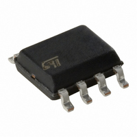
M24C01-WMN6P STMicroelectronics, M24C01-WMN6P Datasheet - Page 16

M24C01-WMN6P
Manufacturer Part Number
M24C01-WMN6P
Description
IC EEPROM 1KBIT 400KHZ 8SOIC
Manufacturer
STMicroelectronics
Datasheets
1.M24C01-WMN6TP.pdf
(39 pages)
2.M24C04-WMN6P.pdf
(29 pages)
3.M24C01-WMN6P.pdf
(40 pages)
Specifications of M24C01-WMN6P
Format - Memory
EEPROMs - Serial
Memory Type
EEPROM
Memory Size
1K (128 x 8)
Speed
400kHz
Interface
I²C, 2-Wire Serial
Voltage - Supply
2.5 V ~ 5.5 V
Operating Temperature
-40°C ~ 85°C
Package / Case
8-SOIC (3.9mm Width)
Organization
128 K x 8
Interface Type
I2C
Maximum Clock Frequency
0.4 MHz
Access Time
900 ns
Supply Voltage (max)
5.5 V
Supply Voltage (min)
2.5 V
Maximum Operating Current
2 mA
Maximum Operating Temperature
+ 85 C
Mounting Style
SMD/SMT
Minimum Operating Temperature
- 40 C
Operating Supply Voltage
2.5 V, 5.5 V
Memory Configuration
128 X 8
Clock Frequency
400kHz
Supply Voltage Range
2.5V To 5.5V
Memory Case Style
SOIC
No. Of Pins
8
Rohs Compliant
Yes
Density
1Kb
Access Time (max)
900ns
Frequency (max)
400KHz
Write Protection
Yes
Data Retention
40Year
Operating Supply Voltage (typ)
3.3/5V
Package Type
SOIC
Operating Temp Range
-40C to 85C
Supply Current
2mA
Operating Supply Voltage (min)
2.5V
Operating Supply Voltage (max)
5.5V
Operating Temperature Classification
Industrial
Mounting
Surface Mount
Pin Count
8
Lead Free Status / RoHS Status
Lead free / RoHS Compliant
Other names
497-8558
M24C01-WMN6P
M24C01-WMN6P
Available stocks
Company
Part Number
Manufacturer
Quantity
Price
Device operation
3.7
3.7.1
16/39
Figure 10. Read mode sequences
1. The seven most significant bits of the device select code of a Random Read (in the 1
Read operations
Read operations are performed independently of the state of the Write Control (WC) signal.
The device has an internal address counter which is incremented each time a byte is read.
Random Address Read
A dummy Write is first performed to load the address into this address counter (as shown in
Figure
condition, and repeats the device select code, with the Read/Write bit (RW) set to 1. The
device acknowledges this, and outputs the contents of the addressed byte. The bus master
must not acknowledge the byte, and terminates the transfer with a Stop condition.
be identical.
10) but without sending a Stop condition. Then, the bus master sends another Start
Current
Address
Read
Random
Address
Read
Sequentila
Current
Read
Sequential
Random
Read
Dev select *
Dev select *
Dev select
Dev select
ACK
Doc ID 5067 Rev 16
Data out N
R/W
R/W
R/W
R/W
ACK
ACK
ACK
ACK
NO ACK
Byte address
Byte address
Data out 1
Data out
M24C16, M24C08, M24C04, M24C02, M24C01
NO ACK
ACK
ACK
ACK
Dev select *
Dev select *
ACK
ACK
ACK
R/W
R/W
Data out N
Data out 1
Data out
st
and 3
NO ACK
NO ACK
rd
ACK
AI01942b
bytes) must


