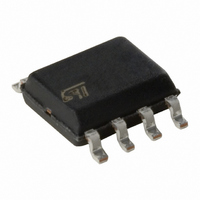
M24C32-WMN6P STMicroelectronics, M24C32-WMN6P Datasheet - Page 14

M24C32-WMN6P
Manufacturer Part Number
M24C32-WMN6P
Description
IC EEPROM 32KBIT 400KHZ 8SOIC
Manufacturer
STMicroelectronics
Specifications of M24C32-WMN6P
Format - Memory
EEPROMs - Serial
Memory Type
EEPROM
Memory Size
32K (4K x 8)
Speed
400kHz
Interface
I²C, 2-Wire Serial
Voltage - Supply
2.5 V ~ 5.5 V
Operating Temperature
-40°C ~ 85°C
Package / Case
8-SOIC (3.9mm Width)
Organization
4 K x 8
Interface Type
I2C
Maximum Clock Frequency
0.4 MHz
Access Time
900 ns
Supply Voltage (max)
5.5 V
Supply Voltage (min)
2.5 V
Maximum Operating Current
2 mA
Maximum Operating Temperature
+ 85 C
Mounting Style
SMD/SMT
Minimum Operating Temperature
- 40 C
Operating Supply Voltage
2.5 V, 5.5 V
Memory Configuration
4096 X 8
Clock Frequency
400kHz
Supply Voltage Range
2.5V To 5.5V
Memory Case Style
SO
No. Of Pins
8
Rohs Compliant
Yes
Lead Free Status / RoHS Status
Lead free / RoHS Compliant
Other names
497-8572
M24C32-WMN6P
M24C32-WMN6P
Available stocks
Company
Part Number
Manufacturer
Quantity
Price
Company:
Part Number:
M24C32-WMN6P
Manufacturer:
STM
Quantity:
553
Part Number:
M24C32-WMN6P
Manufacturer:
STM
Quantity:
20 000
Device operation
4.5
14/38
Memory addressing
To start communication between the bus master and the slave device, the bus master must
initiate a Start condition. Following this, the bus master sends the device select code, shown
in
The device select code consists of a 4-bit device type identifier, and a 3-bit Chip Enable
“Address” (E2, E1, E0). To address the memory array, the 4-bit device type identifier is
1010b.
Up to eight memory devices can be connected on a single I
unique 3-bit code on the Chip Enable (E0, E1, E2) inputs. When the device select code is
received, the device only responds if the Chip Enable Address is the same as the value on
the Chip Enable (E0, E1, E2) inputs.
The 8
If a match occurs on the device select code, the corresponding device gives an
acknowledgment on Serial Data (SDA) during the 9
the device select code, it deselects itself from the bus, and goes into Standby mode.
Table 5.
1. X =
Current Address
Read
Random Address
Read
Sequential Read
Byte Write
Page Write
Table 2
th
Mode
V
IH
bit is the Read/Write bit (RW). This bit is set to 1 for Read and 0 for Write operations.
or V
(on Serial Data (SDA), most significant bit first).
IL
Operating modes
.
RW bit WC
1
0
1
1
0
0
V
V
X
X
X
X
IL
IL
(1)
Doc ID 4578 Rev 17
Bytes
32
1
1
1
1
th
Start, device select, RW = 1
Start, device select, RW = 0, Address
reStart, device select, RW = 1
Similar to Current or Random Address
Read
Start, device select, RW = 0
Start, device select, RW = 0
bit time. If the device does not match
M24C32-W M24C32-R M24C32-F
2
C bus. Each one is given a
Initial sequence


