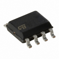
M95040-RMN6P STMicroelectronics, M95040-RMN6P Datasheet - Page 20

M95040-RMN6P
Manufacturer Part Number
M95040-RMN6P
Description
IC EEPROM 4KBIT 5MHZ 8SOIC
Manufacturer
STMicroelectronics
Datasheet
1.M95010-WMN6TP.pdf
(43 pages)
Specifications of M95040-RMN6P
Format - Memory
EEPROMs - Serial
Memory Type
EEPROM
Memory Size
4K (512 x 8)
Speed
5MHz
Interface
SPI, 3-Wire Serial
Voltage - Supply
1.8 V ~ 5.5 V
Operating Temperature
-40°C ~ 85°C
Package / Case
8-SOIC (3.9mm Width)
Lead Free Status / RoHS Status
Lead free / RoHS Compliant
Other names
497-8602-5
M95040-RMN6P
M95040-RMN6P
Available stocks
Company
Part Number
Manufacturer
Quantity
Price
Instructions
6.4
20/43
Write Status Register (WRSR)
The Write Status Register (WRSR) instruction allows new values to be written to the Status
register. Before it can be accepted, a Write Enable (WREN) instruction must previously have
been executed.
The Write Status Register (WRSR) instruction is entered by driving Chip Select (S) low,
sending the instruction code followed by the data byte on Serial Data input (D), and driving
the Chip Select (S) signal high. Chip Select (S) must be driven high after the rising edge of
Serial Clock (C) that latches in the eighth bit of the data byte, and before the next rising edge
of Serial Clock (C). Otherwise, the Write Status Register (WRSR) instruction is not
executed.
Driving the Chip Select (S) signal high at a byte boundary of the input data triggers the self-
timed write cycle that takes t
instruction sequence is shown in
While the Write Status Register cycle is in progress, the Status register may still be read to
check the value of the Write in progress (WIP) bit: the WIP bit is 1 during the self-timed write
cycle t
reset at the end of the write cycle t
The Write Status Register (WRSR) instruction allows the user to change the values of the
BP1, BP0 bits which define the size of the area that is to be treated as read only, as defined
in
The contents of the BP1, BP0 bits are updated after the completion of the WRSR
instruction, including the t
The Write Status Register (WRSR) instruction has no effect on the b7, b6, b5, b4, b1 and b0
bits in the Status register. Bits b7, b6, b5, b4 are always read as 0.
Figure 10. Write Status Register (WRSR) sequence
The instruction is not accepted, and is not executed, under the following conditions:
●
●
●
●
Table
if the Write Enable Latch (WEL) bit has not been set to 1 (by executing a Write Enable
instruction just before)
if a write cycle is already in progress
if the device has not been deselected, by Chip Select (S) being driven high, after the
eighth bit, b0, of the data byte has been latched in
if Write Protect (W) is low during the WRSR command (instruction, address and data)
W
, and, 0 when the write cycle is complete. The WEL bit (Write enable latch) is also
3.
S
C
D
Q
0
1
W
High Impedance
write cycle.
2
W
Instruction
to complete (as specified in
Doc ID 6512 Rev 8
3
Figure
4
W
.
5
6
10.
7
MSB
7
8
6
9 10 11 12 13 14 15
5
Register In
4
Status
3
Table 13
2
1
M95040, M95020, M95010
0
to
AI01445B
Table
20). The


