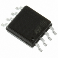
M95256-WMW6TG STMicroelectronics, M95256-WMW6TG Datasheet - Page 20

M95256-WMW6TG
Manufacturer Part Number
M95256-WMW6TG
Description
IC EEPROM 256KBIT 5MHZ 8SOIC
Manufacturer
STMicroelectronics
Datasheet
1.M95256-WMN6TP.pdf
(47 pages)
Specifications of M95256-WMW6TG
Format - Memory
EEPROMs - Serial
Memory Type
EEPROM
Memory Size
256K (32K x 8)
Speed
5MHz
Interface
SPI, 3-Wire Serial
Voltage - Supply
2.5 V ~ 5.5 V
Operating Temperature
-40°C ~ 85°C
Package / Case
8-SOIC (5.3mm Width), 8-SOP, 8-SOEIAJ
Lead Free Status / RoHS Status
Lead free / RoHS Compliant
Other names
497-8692-2
M95256-WMW6TG
M95256-WMW6TG
Available stocks
Company
Part Number
Manufacturer
Quantity
Price
Company:
Part Number:
M95256-WMW6TG
Manufacturer:
ST
Quantity:
4 300
Part Number:
M95256-WMW6TG
Manufacturer:
ST
Quantity:
20 000
Instructions
5.6
Note:
20/47
Figure 10. Read from Memory Array (READ) sequence
1. The most significant address bit (b15) is Don’t Care.
Write to Memory Array (WRITE)
As shown in
low. The bits of the instruction byte, address bytes, and at least one data byte are then
shifted in, on Serial Data input (D). The instruction is terminated by driving Chip Select (S)
high at a byte boundary of the input data. The self-timed Write cycle, triggered by the rising
edge of Chip Select (S), continues for a period t
Table 19
In the case of
has been latched in, indicating that the instruction is being used to write a single byte. If,
though, Chip Select (S) continues to be driven low, as shown in
input data is shifted in, so that more than a single byte, starting from the given address
towards the end of the same page, can be written in a single internal Write cycle.
Each time a new data byte is shifted in, the least significant bits of the internal address
counter are incremented. If the number of data bytes sent to the device exceeds the page
boundary, the internal address counter rolls over to the beginning of the page, and the
previous data there are overwritten with the incoming data. (The page size of these devices
is 64 bytes).
The instruction is not accepted, and is not executed, under the following conditions:
●
●
●
●
The self-timed Write cycle t
events: [Erase addressed byte(s)], followed by [Program addressed byte(s)]. An erased bit is
read as “0” and a programmed bit is read as “1”.
S
C
D
Q
if the Write Enable Latch (WEL) bit has not been set to 1 (by executing a Write Enable
instruction just before)
if a Write cycle is already in progress
if the device has not been deselected, by Chip Select (S) being driven high, at a byte
boundary (after the eighth bit, b0, of the last data byte that has been latched in)
if the addressed page is in the region protected by the Block Protect (BP1 and BP0)
bits.
and
Figure
0
Table
Figure
1
High Impedance
2
Instruction
20.), at the end of which the Write in Progress (WIP) bit is reset to 0.
11, to send this instruction to the device, Chip Select (S) is first driven
11, Chip Select (S) is driven high after the eighth bit of the data byte
3
4
W
5
is internally executed as a sequence of two consecutive
Doc ID 12276 Rev 13
6
7
MSB
15
8
14 13
9 10
16-Bit Address
M95256-DR, M95256, M95256-W, M95256-R
3
20 21 22 23 24 25 26 27
WC
2
(as specified in
1
0
MSB
7
6
Figure
5
Data Out 1
Table
4
3
28 29 30
12, the next byte of
17,
2
1
Table
0
31
7
AI01793D
Data Out 2
18,


