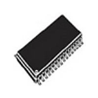
R1LP0408CSB-5SC#S0 Renesas Electronics America, R1LP0408CSB-5SC#S0 Datasheet - Page 14

R1LP0408CSB-5SC#S0
Manufacturer Part Number
R1LP0408CSB-5SC#S0
Description
IC SRAM 4MBIT 55NS 32TSOP
Manufacturer
Renesas Electronics America
Datasheet
1.R1LP0408CSP-5SCB0.pdf
(16 pages)
Specifications of R1LP0408CSB-5SC#S0
Format - Memory
RAM
Memory Type
SRAM
Memory Size
4M (512K x 8)
Speed
55ns
Interface
Parallel
Voltage - Supply
4.5 V ~ 5.5 V
Operating Temperature
-20°C ~ 70°C
Package / Case
32-TSOP II
Density
4Mb
Access Time (max)
55ns
Sync/async
Asynchronous
Architecture
Not Required
Clock Freq (max)
Not RequiredMHz
Operating Supply Voltage (typ)
5V
Address Bus
19b
Package Type
TSOP-II
Operating Temp Range
-20C to 70C
Number Of Ports
1
Supply Current
3mA
Operating Supply Voltage (min)
4.5V
Operating Supply Voltage (max)
5.5V
Operating Temperature Classification
Commercial
Mounting
Surface Mount
Pin Count
32
Word Size
8b
Number Of Words
512K
Lead Free Status / RoHS Status
Lead free / RoHS Compliant
Other names
R1LP0408CSB5SC#S0
Available stocks
Company
Part Number
Manufacturer
Quantity
Price
R1LP0408C-C Series
Low V
(Ta = −20 to +70°C)
Parameter
V
Data
retention
current
Chip deselect to data retention time
Operation recovery time
Notes: 1. Typical values are at V
Low V
Rev.2.00, May.26.2004, page 12 of 12
CC
0 V
V
2.2 V
V
4.5 V
CS#
CC
DR
for data retention
CC
2. Typical values are at V
3. CS# controls address buffer, WE# buffer, OE# buffer, and Din buffer. In data retention mode,
4. t
CC
Data Retention Timing Waveform (CS# Controlled)
Vin levels (address, WE#, OE#, I/O) can be in the high impedance state.
RC
Data Retention Characteristics
−5SC
−7LC
= read cycle time.
t
CDR
to +70°C
to +40°C
to +25°C
to +70°C
to +40°C
to +25°C
CC
CC
= 3.0 V, Ta = +25°C and specified loading, and not guaranteed.
= 3.0 V, Ta = +40°C and specified loading, and not guaranteed.
Symbol Min Typ
V
I
I
I
I
I
I
t
t
CCDR
CCDR
CCDR
CCDR
CCDR
CCDR
CDR
R
DR
Data retention mode
CS# ≥ V
2
0
t
RC
*
4
CC
1.0*
0.8*
1.0*
0.8*
– 0.2 V
2
1
2
1
Max Unit Test conditions*
8
3
3
16
10
10
V
µA
µA
µA
µA
µA
µA
ns
ns
CS# ≥ V
V
CS# ≥ V
See retention waveform
CC
= 3.0 V, Vin ≥ 0 V
CC
CC
− 0.2 V, Vin ≥ 0 V
− 0.2 V
t
R
3


