N01L63W2AT25I ON Semiconductor, N01L63W2AT25I Datasheet - Page 3
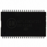
N01L63W2AT25I
Manufacturer Part Number
N01L63W2AT25I
Description
IC SRAM 1MBIT 70NS 44TSOP
Manufacturer
ON Semiconductor
Type
Asynchronousr
Datasheet
1.N01L63W2AB25I.pdf
(10 pages)
Specifications of N01L63W2AT25I
Format - Memory
RAM
Memory Type
SRAM - Asynchronous
Memory Size
1M (64K x 16)
Speed
70ns
Interface
Parallel
Voltage - Supply
2.3 V ~ 3.6 V
Operating Temperature
-40°C ~ 85°C
Package / Case
44-TSOP II
Access Time
30 ns
Supply Voltage (max)
3.6 V
Supply Voltage (min)
2.3 V
Maximum Operating Current
2 mA
Organization
64 K x 16
Maximum Operating Temperature
+ 85 C
Minimum Operating Temperature
- 40 C
Mounting Style
SMD/SMT
Number Of Ports
1
Operating Supply Voltage
3 V
Lead Free Status / RoHS Status
Lead free / RoHS Compliant
Other names
766-1031


Absolute Maximum Ratings
1. Stresses greater than those listed above may cause permanent damage to the device. This is a stress rating only and functional
operation of the device at these or any other conditions above those indicated in the operating section of this specification is not
implied. Exposure to absolute maximum rating conditions for extended periods may affect reliability.
Operating Characteristics (Over Specified Temperature Range)
1. Typical values are measured at Vcc=Vcc Typ., T
2. This parameter is specified with the outputs disabled to avoid external loading effects. The user must add current required to drive
output capacitance expected in the actual system.
3. This device assumes a standby mode if the chip is disabled (CE1 high or CE2 low). In order to achieve low standby current all
inputs must be within 0.2 volts of either VCC or VSS
Read/Write Quiescent Operating Sup-
Page Mode Operating Supply Current
Read/Write Operating Supply Current
Read/Write Operating Supply Current
@ 70ns Cycle Time
Savings with Page Mode Operation
Maximum Data Retention Current
Maximum Standby Current
Voltage on V
Output Leakage Current
Data Retention Voltage
Input Leakage Current
Voltage on any pin relative to V
@ 70 ns Cycle Time
Soldering Temperature and Time
Output High Voltage
@ 1 µs Cycle Time
Output Low Voltage
Input High Voltage
Input Low Voltage
Supply Voltage
ply Current
Operating Temperature
Storage Temperature
diagram)
Power Dissipation
Item
CC
2
Supply Relative to V
(Refer to Power
Item
3
2
2
3
3
1
SS
Symbol
Rev. 9 | Page 3 of 10 | www.onsemi.com
I
I
I
I
V
V
V
I
V
SS
V
I
V
I
CC1
CC2
CC3
CC4
SB1
I
DR
LO
CC
DR
OH
OL
LI
IH
IL
A
=25°C and not 100% tested.
OE = V
Vcc = 1.8V, V
V
V
V
V
Chip Disabled, t
Chip Enabled, I
Chip Enabled, I
Chip Enabled, I
Chip Enabled, I
CC
CC
CC
CC
t
A
= 85
=3.6 V, V
=3.6 V, V
=3.6 V, V
=3.6 V, V
Test Conditions
T
V
Symbol
V
Chip Disabled
V
Chip Disabled
SOLDER
I
IN
T
I
IN,OUT
IH
V
OL
OH
IN
P
T
STG
o
CC
= V
D
A
or Chip Disabled
C, V
= 0 to V
= -0.2mA
= 0.2mA
f = 0
CC
IN
IN
IN
IN
IN
CC
=V
=V
=V
=V
or 0V
= V
OUT
A
OUT
OUT
OUT
= 3.6 V
CC
IH
IH
IH
IH
= 85
CC
3
or V
or V
or V
or V
= 0,
= 0
= 0
= 0
or 0
o
C
IL
IL
IL
IL
–0.3 to V
260
–0.3 to 4.5
–40 to 125
-40 to +85
V
Rating
CC
o
Min.
–0.3
C, 10sec
2.3
1.8
1.8
500
–0.2
CC
+0.3
Typ
3.0
2.0
9.5
2.0
4
1
V
CC
Max
14.0
3.6
0.6
0.2
0.5
0.5
3.0
3.0
20
10
+0.3
Unit
mW
o
o
o
V
V
C
C
C
Unit
mA
mA
mA
mA
µA
µA
µA
µA
V
V
V
V
V
V
Related parts for N01L63W2AT25I
Image
Part Number
Description
Manufacturer
Datasheet
Request
R

Part Number:
Description:
ON Semiconductor [VOLTAGE REGULATOR]
Manufacturer:
ON Semiconductor
Datasheet:
Part Number:
Description:
357-036-542-201 CARDEDGE 36POS DL .156 BLK LOPRO
Manufacturer:
ON Semiconductor
Datasheet:
Part Number:
Description:
357-036-542-201 CARDEDGE 36POS DL .156 BLK LOPRO
Manufacturer:
ON Semiconductor
Datasheet:
Part Number:
Description:
357-036-542-201 CARDEDGE 36POS DL .156 BLK LOPRO
Manufacturer:
ON Semiconductor
Datasheet:
Part Number:
Description:
357-036-542-201 CARDEDGE 36POS DL .156 BLK LOPRO
Manufacturer:
ON Semiconductor
Datasheet:
Part Number:
Description:
357-036-542-201 CARDEDGE 36POS DL .156 BLK LOPRO
Manufacturer:
ON Semiconductor
Datasheet:
Part Number:
Description:
357-036-542-201 CARDEDGE 36POS DL .156 BLK LOPRO
Manufacturer:
ON Semiconductor
Datasheet:
Part Number:
Description:
357-036-542-201 CARDEDGE 36POS DL .156 BLK LOPRO
Manufacturer:
ON Semiconductor
Datasheet:
Part Number:
Description:
357-036-542-201 CARDEDGE 36POS DL .156 BLK LOPRO
Manufacturer:
ON Semiconductor
Datasheet:
Part Number:
Description:
357-036-542-201 CARDEDGE 36POS DL .156 BLK LOPRO
Manufacturer:
ON Semiconductor
Datasheet:
Part Number:
Description:
357-036-542-201 CARDEDGE 36POS DL .156 BLK LOPRO
Manufacturer:
ON Semiconductor
Datasheet:
Part Number:
Description:
Manufacturer:
ON Semiconductor
Datasheet:
Part Number:
Description:
Manufacturer:
ON Semiconductor
Datasheet:
Part Number:
Description:
Manufacturer:
ON Semiconductor
Datasheet: