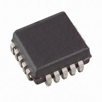
AT17C010-10JI Atmel, AT17C010-10JI Datasheet

AT17C010-10JI
Specifications of AT17C010-10JI
Related parts for AT17C010-10JI
AT17C010-10JI Summary of contents
Page 1
... The AT17 Series Configurators can be programmed with industry-standard program- mers, Atmel’s ATDH2200E Programming Kit or Atmel’s ATDH2225 ISP Cable. ® ™ , APEX ™ ™ ™ ® , XC4000 , XC5200 , Spartan , FPGA Configuration EEPROM Memory 512-kilobit and 1-megabit AT17C512 AT17LV512 AT17C010 AT17LV010 Rev. 0944E–12/01 1 ...
Page 2
Pin Configurations AT17C512/010/LV512/010 2 8-lead LAP DATA 1 8 VCC CLK 2 7 SER_EN RESET/ CEO (A2 GND 8-lead PDIP DATA 1 8 VCC CLK 2 7 SER_EN RESET/ CEO (A2 ...
Page 3
Block Diagram SER_EN WP1 WP2 OSC CONTROL OSC POWER ON RESET CLK READY Device Description 0944E–12/01 PROGRAMMING MODE LOGIC ROW ADDRESS COUNTER BIT COUNTER RESET/OE CE The control signals for the configuration EEPROM (CE, RESET/OE and CCLK) inter- face directly ...
Page 4
Pin Description 8 PDIP/ 20 LAP PLCC Pin Pin Name 1 2 DATA 2 4 CLK (1) 5 WP1 3 6 RESET/OE (1) 7 WP2 GND CEO (1) 15 READY 7 17 ...
Page 5
FPGA Master Serial Mode Summary Control of Configuration Cascading Serial Configuration EEPROMs AT17 Series Reset Polarity Programming Mode Standby Mode 0944E–12/01 The I/O and logic functions of any SRAM-based FPGA are established by a configura- tion program. The program is ...
Page 6
Example Circuits Figure 1. AT17 Series Device for Programming PSLI Devices AT40K/AT40KAL/AT94K RESET RESET GND Notes: 1. Reset polarity must be set to active Low. 2. Use of the optional READY pin is not available on the ...
Page 7
... For details of ISP, please refer to the “Programming Specification for Atmel's AT17 and AT17A Series FPGA Configuration EEPROMs”, available on the Atmel web site, at http://www.atmel.com/atmel/acrobat/doc0437.pdf. Figure 3. In-System Programming of AT17 Series for PSLI Applications AT40K/AT40KAL/AT94K RESET RESET GND Notes: 1. Reset polarity must be set to active Low. ...
Page 8
Absolute Maximum Ratings* Operating Temperature.................................. -55°C to +125°C Storage Temperature ..................................... -65 °C to +150°C Voltage on Any Pin with Respect to Ground ..............................-0. Supply Voltage (V ) .........................................-0.5V to +7.0V CC Maximum Soldering Temp. (10 sec. @ ...
Page 9
DC Characteristics ± 5% Commercial/5V ± 10% Industrial/Military CC Symbol Description V High-level Input Voltage IH V Low-level Input Voltage IL V High-level Output Voltage ( Low-level Output Voltage ( High-level Output Voltage ...
Page 10
AC Characteristics CE RESET/OE CLK T CE DATA AC Characteristics when Cascading RESET/OE CE CLK T CDF LAST BIT DATA T OCK CEO AT17C512/010/LV512/010 10 T SCE CAC T OCE T SCE T ...
Page 11
AC Characteristics for AT17C512/010 ± 5% Commercial ± 10% Industrial/Military CC CC Symbol Description ( Data Delay OE ( Data Delay CE (2) T CLK to Data Delay CAC ...
Page 12
AC Characteristics for AT17LV512/010 V = 3.3V ± 10% CC Symbol Description ( Data Delay OE ( Data Delay CE (2) T CLK to Data Delay CAC T Data Hold From CE, OE, or ...
Page 13
... Package Type Leadless Array Package (LAP) Plastic Dual Inline Package (PDIP) Plastic Leaded Chip Carrier (PLCC) Note: 1. For more information refer to the “Thermal Characteristics of Atmel’s Packages”, available on the Atmel web site, at http://www.atmel.com/atmel/acrobat/doc0636.pdf. 0944E–12/01 AT17C512/010/LV512/010 (1) θ [°C/W] JC 8CN4 ...
Page 14
... Ordering Information – 5V Devices Memory Size Ordering Code 512-Kbit AT17C512-10CC AT17C512-10PC AT17C512-10JC AT17C512-10CI AT17C512-10PI AT17C512-10JI 1-Mbit AT17C010-10CC AT17C010-10PC AT17C010-10JC AT17C010-10CI AT17C010-10PI AT17C010-10JI Ordering Information – 3.3V Devices Memory Size Ordering Code 512-Kbit AT17LV512-10CC AT17LV512-10PC AT17LV512-10JC AT17LV512-10CI AT17LV512-10PI AT17LV512-10JI 1-Mbit AT17LV010-10CC AT17LV010-10PC AT17LV010-10JC AT17LV010-10CI ...
Page 15
Packaging Information 8CN4 – LAP Marked Pin1 Indentifier E 0.10 mm TYP Bottom View Note: 1. Metal Pad Dimensions. 1150 E.Cheyenne Mtn Blvd. Colorado Springs, CO 80906 R 0944E–12/01 D Top View Side View ...
Page 16
PDIP A SEATING PLANE Notes: 1. This package conforms to JEDEC reference MS-001 BA. 2. Dimensions D and E1 do not include mold Flash or Protrusion. Mold Flash or Protrusion shall not exceed 0.25 mm ...
Page 17
PLCC 1.14(0.045) X 45˚ B 0.51(0.020)MAX 45˚ MAX (3X) Notes: 1. This package conforms to JEDEC reference MS-018, Variation AA. 2. Dimensions D1 and E1 do not include mold protrusion. Allowable protrusion is .010"(0.254 mm) per side. Dimension ...
Page 18
... No licenses to patents or other intellectual property of Atmel are granted by the Company in connection with the sale of Atmel products, expressly or by implication. Atmel’s products are not authorized for use as critical components in life support devices or systems. ...


