DS1216F Maxim Integrated Products, DS1216F Datasheet - Page 3
DS1216F
Manufacturer Part Number
DS1216F
Description
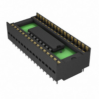
IC SMART/ROM 3V 64/256/1M 32SOIC
Manufacturer
Maxim Integrated Products
Datasheet
1.DS1216C.pdf
(14 pages)
Specifications of DS1216F
Controller Type
Smartwatch ROM
Voltage - Supply
4.5 V ~ 5.5 V
Operating Temperature
0°C ~ 70°C
Package / Case
32-DIP (0.600", 15.24mm) Socket
Lead Free Status / RoHS Status
Contains lead / RoHS non-compliant
Available stocks
Company
Part Number
Manufacturer
Quantity
Price


DE AILED DESC
The DS1216 SmartWatch RA
built-in CMOS watch function, an N
The sockets provide an NV RAM so
from 26 pins to
problems associated with memory vola
The SmartWatch ROM sockets use the embedded lithium source to maintain the time and date only. A
key feature of the SmartWatch is that the watch function remains transparent to the RAM. The
SmartWatch monitors V
lithium energy source is automatically switched on and write protection is unconditionally enabled to
prevent loss of watch and RAM data.
Using
take up no more area than the m mory alone. The Sm rtWatch uses the V
for RAM and watch control. All other pins are passed straight through to the socket receptacle.
The S
hours, days, date, months, and years. The date at
months with fewer than 31 days, including correction for leap years. The SmartWatch operates in either
24-hour or 12-hour format with an AM/PM indicato
OPERATION
Communica
64 bits that must be matched by executing 64 consecutive write cycles containing the proper data on
DQ0. On the SmartWatch ROM, communication with the clock is established using A2 and A0, and
either OE or CE. All
After the pattern m
disabled. Once the pa
registers. When power is cycled, 64 reads should be executed prior to any writes to ensure that the RTC
r
during the match s
sequence.
PATTERN MATCH—RAM
Data transfer to and from the timekeeping registers is accomplished with a serial bit stream under control
of chip enable (CE), output enable (OE), and write enable (WE). Initially, a read cycle to any memory
location using the CE and OE control of the SmartWatch starts the pattern recognition sequence by
moving a pointer to the first bit of the 64-bit comparison register. Next, 64 consecutive write cycles are
executed using the CE and WE control of the SmartWatch. These 64 write cycles are used only to gain
access to the SmartWatch. Therefore, any address to the memory in the socket is acceptable. However,
the write cycles generated to gain access to the SmartWatch are also writing data to a location in the
mated RAM. The preferred way to manage this requirement is to set aside just one address location in
RAM as a SmartWatch scratch pad. When the first write cycle is executed, it is compared to bit 0 of the
64-bit comparison register. If a match is found, the pointer increments to the next location of the
egisters a
T
martWatch pr
the SmartWa
re not w
tion with the SmartW
32 pins. When a socket is m
equen
ritten.
tch saves P
ovides tim
atch, the nex
accesses that occur prior to recognition of the 64-bit pattern are directed to memory.
ttern is e
RIPTION
C
ce. A patte
C
A pattern
for an out-of-tolerance condition. When such a condition occurs, an internal
M and Smart
ekeeping
C board
e
s
tablished, the next
atch RAM is estab
t 64 reads an
rn match
match is
lution f
V RAM
tility and uses a common energy source to maintain time and date.
space since
information
or memory sized from 2k x 8 to 51
ated with a CMOS SRAM, it provi
Watch ROM Sockets are 600-
is also terminated
controller circuit, and an embedded
ignored if the RST
d/or w
3 of 14
r.
the com
lished by pattern rec
th
in
a
64 re
e end of the m
cluding hundre
rites are directed to the cl
ad/write cycles will be direc
bination o
DS1216 SmartWatch RAM/SmartWatch ROM
if a ea
bit is zero and th
r
f Smar
dth
onth i
d occurs during the 64-bit match
ognition on a serial bit stream of
s of seconds, seconds, minutes,
CC
mil-wide DIP sockets with a
, data I/O 0, CE, OE, and WE
s automatically adjusted for
tWatch and the mated RAM
des a complete solution to
2k x 8 with package sizes
lithium energy source.
ock, and the RAM is
e RST pin goes low
ted to the RTC
Related parts for DS1216F
Image
Part Number
Description
Manufacturer
Datasheet
Request
R

Part Number:
Description:
MAX7528KCWPMaxim Integrated Products [CMOS Dual 8-Bit Buffered Multiplying DACs]
Manufacturer:
Maxim Integrated Products
Datasheet:
Part Number:
Description:
Single +5V, fully integrated, 1.25Gbps laser diode driver.
Manufacturer:
Maxim Integrated Products
Datasheet:
Part Number:
Description:
Single +5V, fully integrated, 155Mbps laser diode driver.
Manufacturer:
Maxim Integrated Products
Datasheet:
Part Number:
Description:
VRD11/VRD10, K8 Rev F 2/3/4-Phase PWM Controllers with Integrated Dual MOSFET Drivers
Manufacturer:
Maxim Integrated Products
Datasheet:
Part Number:
Description:
Highly Integrated Level 2 SMBus Battery Chargers
Manufacturer:
Maxim Integrated Products
Datasheet:
Part Number:
Description:
Current Monitor and Accumulator with Integrated Sense Resistor; ; Temperature Range: -40°C to +85°C
Manufacturer:
Maxim Integrated Products
Part Number:
Description:
TSSOP 14/A°/RS-485 Transceivers with Integrated 100O/120O Termination Resis
Manufacturer:
Maxim Integrated Products
Part Number:
Description:
TSSOP 14/A°/RS-485 Transceivers with Integrated 100O/120O Termination Resis
Manufacturer:
Maxim Integrated Products
Part Number:
Description:
QFN 16/A°/AC-DC and DC-DC Peak-Current-Mode Converters with Integrated Step
Manufacturer:
Maxim Integrated Products
Part Number:
Description:
TDFN/A/65V, 1A, 600KHZ, SYNCHRONOUS STEP-DOWN REGULATOR WITH INTEGRATED SWI
Manufacturer:
Maxim Integrated Products
Part Number:
Description:
Integrated Temperature Controller f
Manufacturer:
Maxim Integrated Products
Part Number:
Description:
SOT23-6/I°/45MHz to 650MHz, Integrated IF VCOs with Differential Output
Manufacturer:
Maxim Integrated Products
Part Number:
Description:
SOT23-6/I°/45MHz to 650MHz, Integrated IF VCOs with Differential Output
Manufacturer:
Maxim Integrated Products
Part Number:
Description:
EVALUATION KIT/2.4GHZ TO 2.5GHZ 802.11G/B RF TRANSCEIVER WITH INTEGRATED PA
Manufacturer:
Maxim Integrated Products
Part Number:
Description:
QFN/E/DUAL PCIE/SATA HIGH SPEED SWITCH WITH INTEGRATED BIAS RESISTOR
Manufacturer:
Maxim Integrated Products
Datasheet: