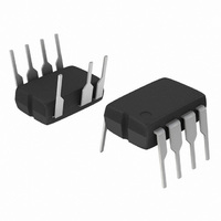
NCP1216AP100G ON Semiconductor, NCP1216AP100G Datasheet - Page 5

NCP1216AP100G
Manufacturer Part Number
NCP1216AP100G
Description
IC CTRLR PWM CM OTP HV 8DIP
Manufacturer
ON Semiconductor
Datasheet
1.NCP1216AP100G.pdf
(18 pages)
Specifications of NCP1216AP100G
Output Isolation
Isolated
Frequency Range
90 ~ 110kHz
Voltage - Input
10 ~ 16 V
Operating Temperature
0°C ~ 150°C
Package / Case
8-DIP (0.300", 7.62mm), 7 Leads
Duty Cycle (max)
50 %
Mounting Style
Through Hole
Switching Frequency
110 KHz
Maximum Operating Temperature
+ 150 C
Fall Time
20 ns
Rise Time
60 ns
Synchronous Pin
No
Topology
Flyback
Lead Free Status / RoHS Status
Lead free / RoHS Compliant
Available stocks
Company
Part Number
Manufacturer
Quantity
Price
Company:
Part Number:
NCP1216AP100G
Manufacturer:
ON Semiconductor
Quantity:
1 700
Part Number:
NCP1216AP100G
Manufacturer:
ON/安森美
Quantity:
20 000
4. A 1.0 MW resistor is connected to the ground for the measurement.
ELECTRICAL CHARACTERISTICS
T
INTERNAL OSCILLATOR (V
FEEDBACK SECTION (V
SKIP CYCLE GENERATION
INTERNAL RAMP COMPENSATION
Oscillation Frequency, 65 kHz Version
Oscillation Frequency, 100 kHz Version
Oscillation Frequency, 133 kHz Version
Built−in Frequency Jittering in Percentage of f
Maximum Duty−Cycle
Internal Pullup Resistor
Pin 2 (FB) to Internal Current Setpoint Division Ratio
Default Skip Mode Level
Pin 1 Internal Output Impedance
Internal Ramp Level @ 25°C (Note 4)
Internal Ramp Resistance to C
J
= 150°C, V
CC
= 11 V unless otherwise noted.)
CC
CC
= 11 V, Pin 5 Loaded by 1.0 kW)
S
= 11 V, Pin 5 Loaded by 1.0 kW)
Characteristic
Pin
(continued) (For typical values T
OSC
http://onsemi.com
5
NCP1216A
NCP1216
J
= 25°C, for min/max values T
Pin
2
−
1
1
3
3
Symbol
R
V
D
V
f
f
f
f
I
Z
R
OSC
OSC
OSC
jitter
ratio
ramp
ramp
max
skip
out
up
58.5
Min
120
0.9
2.6
90
69
42
J
= 0°C to +125°C, Maximum
±4.0
46.5
Typ
100
133
3.3
1.1
2.9
65
75
20
25
19
Max
71.5
1.26
110
146
3.2
81
50
Unit
kHz
kHz
kHz
kW
kW
kW
%
%
V
V


