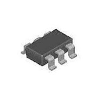
SGP400TZ Fairchild Semiconductor, SGP400TZ Datasheet - Page 10

SGP400TZ
Manufacturer Part Number
SGP400TZ
Description
IC CTRLR PWM GREEN CM OTP SSOT6
Manufacturer
Fairchild Semiconductor
Datasheet
1.SGP400TZ.pdf
(15 pages)
Specifications of SGP400TZ
Output Isolation
Isolated
Frequency Range
62 ~ 68kHz
Voltage - Input
8 ~ 30 V
Voltage - Output
18V
Power (watts)
247mW
Operating Temperature
-40°C ~ 125°C
Package / Case
6-SSOT, SuperSOT™-6
Output Voltage
1.5 V to 8 V
Input Voltage
0.3 V to 7 V
Switching Frequency
68 KHz
Operating Temperature Range
- 20 C to + 85 C
Mounting Style
SMD/SMT
Duty Cycle (max)
80 %
Number Of Outputs
1
Lead Free Status / RoHS Status
Lead free / RoHS Compliant
Low-Power Green-Mode PWM Flyback Power Controller without Secondary Feedback
Constant Output Power Limit
When the SENSE voltage across the sense resistor, R
reaches the threshold voltage (around 1.0V), the output
GATE drive is turned off after a small propagation
delay t
current, proportional to t
delay is nearly constant, regardless of the input line
voltage V
additional currents. Under high input-line voltages,
the output power limit is higher than under low
input-line voltages.
Over a wide range of AC input voltages, the variation
can be significant. To compensate for this, the
threshold voltage is adjusted by adding a positive ramp
(V
1.05V and it flattens out at 1.05V. A smaller threshold
voltage forces the output GATE drive to terminate
earlier, reducing total PWM turn-on time and making
the output power equal to that of the low line input.
This proprietary internal compensation feature ensures
a constant output power limit over a wide range of AC
input voltages (90V
Under-voltage Lockout (UVLO)
The turn-on/turn-off thresholds are fixed internally at
17V/8V. To enable the SGP400 during start-up, the
hold-up capacitor must first be charged to 17V through
the start-up resistor.
The hold-up capacitor continues to supply V
energy can be delivered from the auxiliary winding of
the main transformer. V
during this start-up process. This UVLO hysteresis
window ensures that the hold-up capacitor can
adequately supply V
© System General Corp.
Version 1.0.1 (IAO33.0084.B0)
LIMIT_RAMP
PD
. This propagation delay introduces additional
IN
). This ramp signal can vary from 0.77V to
. Higher input line voltages result in larger
AC
DD
to 264V
during start-up.
DD
PD
must not drop below 8V
•V
AC
IN
).
/L
P
. The propagation
DD
before
S
,
- 10 -
Gate Output
The BiCMOS output stage is a fast totem pole gate
driver. Cross-conduction has been avoided to minimize
heat dissipation, increase efficiency, and enhance
reliability. The output driver is clamped by an internal
17V Zener diode to protect the power MOSFET
transistors against any harmful over-voltage gate signals.
Slope Compensation
The sensed voltage across the current sense resistor is
used for current-mode control and pulse-by-pulse
current limiting. The built-in slope compensation
function improves power supply stability and prevents
sub-harmonic oscillations that normally would occur
because of peak current mode control. A positively
sloped, synchronized ramp is activated with every
switching cycle. The slope of the ramp is:
Noise Immunity
Noise from the current sense or the control signal may
cause significant pulse-width jitter, particularly in
continuous-conduction mode. Slope compensation
helps alleviate this problem. Good placement and
layout practices should be followed. Avoid long PCB
traces and component leads. Compensation and filter
components should be located near the SGP400.
Finally, increasing the power-MOS gate resistance is
advised.
. 0
Duty
33
×
(max)
Duty
www.sg.com.tw • www.fairchildsemi.com
Product Specification
September 24, 2007
SGP400
(1)


