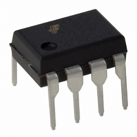
FSQ110 Fairchild Semiconductor, FSQ110 Datasheet - Page 8

FSQ110
Manufacturer Part Number
FSQ110
Description
IC SWIT PWM GREEN CM OVP 8DIP
Manufacturer
Fairchild Semiconductor
Datasheet
1.FSQ110.pdf
(12 pages)
Specifications of FSQ110
Output Isolation
Isolated
Frequency Range
92 ~ 108kHz
Voltage - Input
9 ~ 20 V
Voltage - Output
650V
Power (watts)
12W
Operating Temperature
25°C ~ 140°C
Package / Case
8-DIP (0.300", 7.62mm)
On Resistance (max)
14 Ohms
Maximum Operating Temperature
+ 85 C
Minimum Operating Temperature
- 25 C
Maximum Power Dissipation
1400 mW
Mounting Style
Through Hole
Supply Current
3 mA
Lead Free Status / RoHS Status
Lead free / RoHS Compliant
Available stocks
Company
Part Number
Manufacturer
Quantity
Price
Part Number:
FSQ110
Manufacturer:
FAIRCHILD/ن»™ç«¥
Quantity:
20 000
Part Number:
FSQ110 Q110
Manufacturer:
FAIRCHILD/ن»™ç«¥
Quantity:
20 000
FSQ110 Rev. 1.0.0
© 2007 Fairchild Semiconductor Corporation
Functional Description
1. Startup: In previous generations of Fairchild Power
Switches (FPS™), the Vstr pin required an external
resistor to the DC input voltage line. In this generation,
the startup resistor is replaced by an internal high-
voltage current source and a switch that shuts off 10ms
after the supply voltage, V
source turns back on if V
2. Feedback Control: The FSQ110 employs current-
mode control as shown in Figure 14. An opto-coupler
(such as the H11A817A) and shunt regulator (such as
the KA431) are typically used to implement the feedback
network. Comparing the feedback voltage with the
voltage across the R
offset voltage, makes it possible to control the switching
duty cycle. When the shunt regulator reference pin
voltage exceeds the internal reference voltage of 2.5V,
the opto-coupler LED current increases, the feedback
voltage V
cycle. This typically happens when the input voltage
increases or the output load decreases.
3. Leading-Edge Blanking (LEB): When the internal
SenseFET is turned on, the primary-side capacitance
and secondary-side rectifier diode reverse recovery
typically cause a high-current spike through the
SenseFET. Excessive voltage across the R
leads to incorrect feedback operation in the current-
mode PWM control. To counter this effect, the FPS
employs a Leading-Edge Blanking (LEB) circuit. This
circuit inhibits the PWM comparator for a short time
(t
LEB
V
FSQ110Rev. 1.00
O
) after the SenseFET is turned on.
Figure 14. Pulse Width Modulation Circuit
Figure 13. High-Voltage Current Source
431
FB
is pulled down and thereby reduces the duty
F B
C
V
FB
IN
3
,dc
5μA
V
V
+
-
sense
FB
V
cc
V
SD
CC
D1
CC
V
resistor of SenseFET, plus an
10ms after
CC
UVLO on
UVLO off
V
drops below 8V.
V
V
CC
cc
900μA
FB,in
cc
D2
≥ 12V
<8V
, goes above 12V. The
2.5R
R
FSQ100 Rev. 1.00
I
STR
OSC
I
CH
OLP
V
J-FET
str
driver
sense
Gate
resistor
8
4. Protection Circuits: The FPS has several protective
functions, such as Overload Protection (OLP), Over-
Voltage
(UVLO), and Thermal Shutdown (TSD). Because these
protection circuits are fully integrated in the IC without
external components, reliability is improved without
increasing cost. Once a fault condition occurs, switching
is terminated and the SenseFET remains off. This
causes V
voltage, V
the internal high-voltage current source charges the V
capacitor via the Vstr pin. When V
start voltage, V
normal operation. In this manner, the auto-restart can
alternately enable and disable the switching of the power
SenseFET until the fault condition is eliminated.
4.1 Overload Protection (OLP): Overload is defined as
the load current exceeding a pre-set level due to an
unexpected event. In this situation, the protection circuit
should be activated to protect the SMPS. However, even
when the SMPS is operating normally, the OLP circuit
can be activated during the load transition. To avoid this
undesired operation, the OLP circuit is designed to be
activated after a specified time to determine whether it is
a transient situation or a true overload situation. In
conjunction with the I
current mode feedback path limits the current in the
SenseFET when the maximum PWM duty cycle is
attained. If the output consumes more than this
maximum power, the output voltage (V
below nominal voltage. This reduces the current through
the opto-coupler LED, which also reduces the opto-
coupler transistor current, increasing the feedback
voltage (V
diode is blocked and the 5µA current source (I
starts to slowly charge C
V
operation is terminated, as shown in Figure 15. The
shutdown delay time is the time required to charge C
from 3V to 6V with 5µA current source.
FB
V
6V
3V
FB
increases until it reaches 6V, when the switching
Figure 15. Overload Protection (OLP)
t
CC
Protection
12
STOP
FB
=
). If V
to fall. When V
C
FSQ110 Rev.00
FB
t
1
START
(typically 8V), the protection is reset and
V t
( )
I
2
DELAY
FB
−
V t
(typically 12V), the FPS resumes
(OVP),
PK
( )
exceeds 3V, the feedback input
1
t
12
;
FB
= C
current limit pin (if used), the
I
DELAY
Overload Protection
FB
up to V
CC
×
(V(t
Under-Voltage
=
reaches the UVLO stop
2
)-V(t
5
μ
CC
A V t
CC
1
, ( )
)) / I
reaches the UVLO
. In this condition,
DELAY
1
=
3 , ( )
O
V V t
www.fairchildsemi.com
) decreases
2
Lockout
=
t
2
DELAY
6
V
t
CC
FB
)


