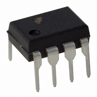
FSQ211 Fairchild Semiconductor, FSQ211 Datasheet - Page 8

FSQ211
Manufacturer Part Number
FSQ211
Description
IC SWIT PWM GREEN UVLO HV 8DIP
Manufacturer
Fairchild Semiconductor
Datasheet
1.FSQ211.pdf
(13 pages)
Specifications of FSQ211
Output Isolation
Isolated
Frequency Range
61 ~ 73kHz
Voltage - Input
8 ~ 20 V
Voltage - Output
650V
Power (watts)
1.4W
Operating Temperature
25°C ~ 145°C
Package / Case
8-DIP (0.300", 7.62mm)
Lead Free Status / RoHS Status
Lead free / RoHS Compliant
Available stocks
Company
Part Number
Manufacturer
Quantity
Price
Part Number:
FSQ211
Manufacturer:
FAIRCHILD/ن»™ç«¥
Quantity:
20 000
© 2007 Fairchild Semiconductor Corporation
FSQ211 Rev. 1.0.0
Functional Description
1. Start-up: At start-up, the internal high-voltage current
source supplies the internal bias and charges the
external V
case of the FSQ211, when V
starts switching and the internal high-voltage current
source stops charging the capacitor. The device is in
normal operation provided V
After start-up, the bias is supplied from the auxiliary
transformer winding.
Calculating the V
design with the FSQ211. At initial start-up, the maximum
value of start operating current I
which supplies current to UVLO and V
charging current I
– 100µA. After V
the bias winding supplies V
When the bias winding voltage is not sufficient, the V
level decreases to the UVLO stop voltage and the
internal current source is activated again to charge the
V
(charging/discharging), the V
chosen with a value between 10µF and 47µF.
V
V
CC
V
Figure 15. Charging V
START
STOP
CC
capacitor.
Figure 14. Internal Start-up Circuit
I
Vcc
CC
I
V
Vcc
= I
UVLO
IN
capacitor, as shown in Figure 14. In the
STR
= I
V
,dc
IN
STR
-I
CC
, dc
START
VCC
CC
-I
To
START
V
reaches the UVLO start voltage, only
CC
capacitor is an important step in a
V
of the V
cc
prevent
9V/7V
I
CC
START
V
CC
CC
CC
Bias winding
Capacitor Through Vstr
CC
CC
below V
UVLO
CC
must not drop
voltage
V
does not drop below 7V.
capacitor is equal to I
I
STR
REF
reaches 9V, the device
current to the device.
this
capacitor should be
STR
L
STOP
Vstr
J-FET
H
is about 100µA,
V
REF
CC
I
STR
Vstr
blocks. The
fluctuation
t
STR
CC
8
2. Feedback Control: The FSQ211 is a voltage-mode
controlled device, as shown in Figure 16. Usually, an
opto-coupler and shunt regulator, like KA431, are used
to implement the feedback network. The feedback
voltage is compared with an internally generated
sawtooth waveform. This directly controls the duty cycle.
When the shunt regulator reference pin voltage exceeds
the internal reference voltage of 2.5V, the opto-coupler
LED current increases, the feedback voltage V
pulled down, and it reduces the duty cycle. This
happens when the input voltage increases or the output
load decreases.
3. Leading Edge Blanking (LEB): The instant the
internal SenseFET is turned on, the primary-side
capacitance and secondary-side rectifier diode reverse
recovery typically cause a high-current spike through the
SenseFET. Excessive voltage across the R
leads to incorrect pulse-by-pulse current limit protection.
To avoid this, a leading edge blanking (LEB) circuit
disables the pulse-by-pulse current limit protection block
for a fixed time (t
4. Protection Circuit: The FSQ211 has several
protective functions, such as overload protection (OLP),
under-voltage lockout (UVLO), and thermal shutdown
(TSD). Because these protection circuits are fully
integrated inside the IC without external components,
reliability is improved without increasing costs. Once a
fault condition occurs, switching is terminated and the
SenseFET remains off. This causes V
V
protection is reset and the internal high-voltage current
source charges the V
V
device resumes normal operation. In this manner, the
auto-restart can alternately enable and disable the
switching of the power SenseFET until the fault
condition is eliminated.
CC
CC
V
o
reaches the UVLO start voltage V
reaches the UVLO stop voltage V
Figure 16. PWM and Feedback Circuit
KA43 1
C
V
fb
fb
4
Figure 17. Protection Block
V
LEB
5µA
C fb
RESE T
fb
) after the SenseFET turns on.
4
V
+
5µA
-
FB
400µA
V
CC
V
SD
R
cc
4.5V
capacitor via the Vstr pin. When
V
ref
OLP
0.40mA
+
-
TSD
OSC
R
OSC
A/R
S
R
S
R
OLP
Q
Q
CC
START
STOP
Protection Block
driver
to fall. When
SENSE
Gate
OLP , TSD
www.fairchildsemi.com
DR IVER
GATE
(7V), the
(9V), the
resistor
FB
is


