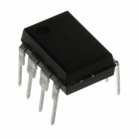
FSFM300N Fairchild Semiconductor, FSFM300N Datasheet - Page 10

FSFM300N
Manufacturer Part Number
FSFM300N
Description
IC SWIT PWM GREEN CM UVLO 8DIP
Manufacturer
Fairchild Semiconductor
Datasheet
1.FSFM300N.pdf
(18 pages)
Specifications of FSFM300N
Output Isolation
Isolated
Frequency Range
61 ~ 73kHz
Voltage - Input
8 ~ 21 V
Voltage - Output
650V
Power (watts)
40W
Operating Temperature
25°C ~ 140°C
Package / Case
8-DIP (0.300", 7.62mm)
Lead Free Status / RoHS Status
Lead free / RoHS Compliant
Available stocks
Company
Part Number
Manufacturer
Quantity
Price
Company:
Part Number:
FSFM300N
Manufacturer:
FAIRCHILD
Quantity:
2 537
FSFM260N / FSFM300N Rev. 1.0.0
© 2009 Fairchild Semiconductor Corporation
Functional Description
1. Startup: In previous generations of Fairchild Power
Switches (FPS™), the V
resistor to the DC input voltage line. In this generation,
the startup resistor is replaced by an internal high-
voltage current source. At startup, an internal high-
voltage current source supplies the internal bias and
charges the external capacitor (C
V
12V, the FSFM260/300 begins switching and the internal
high-voltage current source is disabled. Then, the
FSFM260/300 continues its normal switching operation
and the power is supplied from the auxiliary transformer
winding unless V
2. Feedback Control: FSFM260/300 employs current-
mode control, as shown in Figure 17. An opto-coupler
(such as the FOD817A) and shunt regulator (such as the
KA431) are typically used to implement the feedback
network. Comparing the feedback voltage with the
voltage across the R
control the switching duty cycle. When the reference pin
voltage of the shunt regulator exceeds the internal
reference voltage of 2.5V, the optocoupler LED current
increases, pulling down the feedback voltage and
reducing the duty cycle. This typically occurs when the
input voltage is increased or the output load is
decreased.
2.1 Pulse-by-Pulse Current Limit: Because current-
mode control is employed, the peak current through the
SenseFET is determined by the inverting input of the
PWM comparator (V
the current through the opto-transistor is zero and the
current limit pin (#4) is left floating, the feedback current
source (I
resistor (R+2.5R=2.8k). In this case, the cathode voltage
of diode D2 and the peak drain current have maximum
CC
pin, as illustrated in Figure 16. When V
8V/12V
FB
V
Figure 16. Internal Startup Circuit
CC
) of 0.9mA flows only through the internal
2
CC
goes below the stop voltage of 8V.
FB
SENSE
*), as shown in Figure 17. When
C
Vcc
CC
V
CC
resistor makes it possible to
pin had an external startup
good
vcc
) connected to the
I
FSFM260 Rev: 00
start
Internal
Bias
Vref
CC
V
5
DC
reaches
Vstr
10
values of 2.5V and 1.5A, respectively. The pulse-by-
pulse current limit can be adjusted using a resistor to
GND on the current limit pin (#4). The current limit level
using an external resistor (R
where, I
2.2 Leading-Edge Blanking (LEB): At the instant the
internal SenseFET is turned on, a high-current spike
occurs through the SenseFET, caused by primary-side
capacitance
recovery. Excessive voltage across the R
would lead to incorrect feedback operation in the current-
mode PWM control. To counter this effect, the FSFM260/
300 employs a leading edge blanking (LEB) circuit. This
circuit inhibits the PWM comparator for a short time
(t
2.3 Constant Power Limit Circuit: Due to the circuit
delay of FPS, the pulse-by-pulse limit current increases
a little bit when the input voltage increases. This means
unwanted excessive power is delivered to the secondary
side. To compensate, the auxiliary power compensation
network in Figure 18 can be used. R
by-pulse current by absorbing internal current source
(I
between resistors. With the suggested compensation
circuit, additional current from I
proportionally to the input voltage (V
constant power in wide input range. Choose R
proper current to the application, then check the pulse-
by-pulse current difference between minimum and
maximum input voltage. To eliminate the difference (to
gain constant power), R
V
FSFM260 Rev: 00
I
=>
LEB
FB
R
LIM
O
Figure 17. Pulse Width Modulation (PWM) Circuit
y
: typical value is 0.9mA) depending on the ratio
R
=
≅
) after the SenseFET is turned on.
LIM
R
I
LIM
2
FOD817A
lim_spec
LIM
8 .
=
KA431
I
fb
k
⋅
I
I
Ω
LIM
LIM
I
×
LIM
+
is the desired drain current limit.
_
Vfb
R
ΔI
_
SPEC
LIM
⋅
×
SPEC
. 2
and
lim_comp
V
k 8
dc
−
C
B
Ω
I
LIM
×
3
I
delay
N
N
V
secondary-side
V
SD
a
p
CC
y
D1
can be calculated by:
V
CC
LIM
V
I
FB
D2
+
fb
-
*
) is given by:
2.5R
R
FB
OSC
LIM
is absorbed more
DC
rectifier
OLP
can adjust pulse-
) and achieves
SENSE
www.fairchildsemi.com
driver
Gate
R
SenseFET
sense
reverse
resistor
LIM
(1)
(2)
(3)
for


