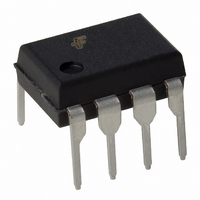
FSQ0170RNA Fairchild Semiconductor, FSQ0170RNA Datasheet - Page 10

FSQ0170RNA
Manufacturer Part Number
FSQ0170RNA
Description
IC SWIT PWM GREEN OVP UVLO 8DIP
Manufacturer
Fairchild Semiconductor
Specifications of FSQ0170RNA
Output Isolation
Isolated
Frequency Range
92 ~ 108kHz
Voltage - Input
8 ~ 20 V
Voltage - Output
700V
Power (watts)
20W
Operating Temperature
25°C ~ 140°C
Package / Case
8-DIP (0.300", 7.62mm)
On Resistance (max)
8.8 Ohms
Maximum Operating Temperature
+ 85 C
Minimum Operating Temperature
- 25 C
Maximum Power Dissipation
1500 mW
Mounting Style
Through Hole
Supply Current
3 mA
Lead Free Status / RoHS Status
Lead free / RoHS Compliant
Available stocks
Company
Part Number
Manufacturer
Quantity
Price
Part Number:
FSQ0170RNA
Manufacturer:
FAIRCHILD/ن»™ç«¥
Quantity:
20 000
FSQ0170RNA, FSQ0270RNA, FSQ0370RNA Rev. 1.0.2
© 2006 Fairchild Semiconductor Corporation
IC to detect the temperature of the SenseFET. When the
temperature exceeds approximately 140°C, thermal
shutdown is activated.
4.3 Over-Voltage Protection (OVP): In the event of a
malfunction in the secondary-side feedback circuit, or an
open feedback loop caused by a soldering defect, the
current through the opto-coupler transistor becomes
almost zero (see Figure 14). V
manner to the overload situation, forcing the preset
maximum current to be supplied to the SMPS until the
overload protection is activated. Because excess energy
is provided to the output, the output voltage may exceed
the rated voltage before the overload protection is
activated, resulting in the breakdown of the devices in
the secondary side. To prevent this situation, an Over-
Voltage Protection (OVP) circuit is employed. In general,
V
uses V
voltage. If V
resulting in termination of the switching operation. To
avoid undesired activation of OVP during normal
operation, V
5. Soft-Start: The FPS has an internal soft-start circuit
that slowly increases the SenseFET current after start-
up, as shown in Figure 16. The typical soft-start time is
10ms, where progressive increments of the SenseFET
current are allowed during the start-up phase. The pulse
width to the power switching device is progressively
increased to establish the correct working conditions for
transformers, inductors, and capacitors. The voltage on
the output capacitors is progressively increased to
smoothly establish the required output voltage. This also
helps prevent transformer saturation and reduces the
stress on the secondary diode during startup.
6. Burst Operation: To minimize power dissipation in
standby mode, the FPS enters burst-mode operation.
Feedback voltage decreases as the load decreases, as
shown in Figure 17, and the device automatically enters
burst-mode when the feedback voltage drops below
V
feedback voltage drops below V
CC
BURH
is proportional to the output voltage and the FPS
(typically 600mV). Switching continues until the
CC
CC
instead of directly monitoring the output
CC
Figure 16. Soft-Start Function
exceeds 19V, the OVP circuit is activated,
should be designed to be below 19V.
5V
I
LIM
FSQ0x70RNA Rev. 1.00
FB
BURL
R
sense
climbs up in a similar
(typically 400mV).
#6,7,8
DRAIN
GND
#1
10
At this point, switching stops and the output voltage
starts to drop at a rate dependent on the standby current
load. This causes the feedback voltage to rise. Once it
passes V
voltage then falls and the process is repeated. Burst-
mode operation alternately enables and disables
switching of the SenseFET and reduces switching loss in
standby mode.
7. Adjusting Peak Current Limit: As shown in Figure
18, a combined 2.8kΩ internal resistance is connected to
the non-inverting lead on the PWM comparator. An
external resistance of Rx on the current limit pin forms a
parallel resistance with the 2.8kΩ when the internal
diodes are biased by the main current source of 900µA.
For example, FSQ0270RNA has a typical SenseFET
peak current limit (I
0.6A by inserting Rx between the I
The value of the Rx can be estimated by the following
equations:
0.9A: 0.6A = 2.8kΩ : XkΩ,
X = Rx || 2.8kΩ
where X represents the resistance of the parallel network.
Waveform
V
V
Rx
Current
BURH
BURL
Figure 18. Peak Current Limit Adjustment
V
FB
Figure 17. Burst Operation Function
V
I
PK
FB
BURH
3
4
I
DELAY
Burst Operation
, switching resumes. The feedback
V
CC
5
Switching OFF
μ
LIM
A
I
) of 0.9A. I
FB
V
CC
900
Burst Operation
μ
A
0.8k
2k
LIM
PK
Ω
Ω
Switching
FSQ0x70RNA Rev. 1.00
pin and the ground.
can be adjusted to
OFF
FSQ0x70RNA Rev.00
Comparator
www.fairchildsemi.com
PWM
SenseFET
Current
Operation
Sense
Normal


