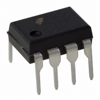
FSQ0370RNA Fairchild Semiconductor, FSQ0370RNA Datasheet - Page 5

FSQ0370RNA
Manufacturer Part Number
FSQ0370RNA
Description
IC SWIT PWM GREEN OVP UVLO 8DIP
Manufacturer
Fairchild Semiconductor
Series
FPS™r
Specifications of FSQ0370RNA
Output Isolation
Isolated
Frequency Range
92kHz ~ 108kHz
Voltage - Input
9 V ~ 20 V
Voltage - Output
700V
Power (watts)
27W
Operating Temperature
25°C ~ 140°C
Package / Case
8-DIP (0.300", 7.62mm)
Power Switch Family
FSQ0370
Power Switch On Resistance
4Ohm
Output Current
970mA
Number Of Outputs
Single
Mounting
Through Hole
Supply Current
3mA
Package Type
PDIP
Operating Temperature (min)
-25C
Operating Temperature (max)
85C
Operating Temperature Classification
Commercial
Pin Count
8
Power Dissipation
1.5W
On Resistance (max)
4 Ohms
Maximum Operating Temperature
+ 85 C
Minimum Operating Temperature
- 25 C
Maximum Power Dissipation
1500 mW
Mounting Style
Through Hole
Lead Free Status / RoHS Status
Lead free / RoHS Compliant
Available stocks
Company
Part Number
Manufacturer
Quantity
Price
Company:
Part Number:
FSQ0370RNA
Manufacturer:
FSC
Quantity:
81 000
Part Number:
FSQ0370RNA
Manufacturer:
FAIRCHILD/ن»™ç«¥
Quantity:
20 000
HCPL062N Rev. 1.0.0
Transfer Characteristics
Isolation Characteristics
Notes:
3. All typical values are at V
4. t
5. t
6. t
7. t
8. CM
9. CM
10. Device considered a two-terminal device: Pins 1,2,3 and 4 shorted together, and Pins 5,6,7 and 8 shorted together.
11. The power supply bypass capacitors must be no further than 3mm from the leads of the optocoupler. A low
Symbol
Symbol
V
pulse to the 1.5V level on the LOW to HIGH transition of the output voltage pulse.
pulse to the 1.5V level on the HIGH to LOW transition of the output voltage pulse.
state (i.e., V
output state (i.e., V
inductance ground plane width of with ≤ 5nHy of series lead inductance is required.
I
V
PLH
PHL
r
f
R
C
FT
I
OL
– Fall time is measured from the 10% to the 90% levels on the HIGH to LOW transition of the output pulse.
I-O
– Rise time is measured from the 90% to the 10% levels on the LOW to HIGH transition of the output pulse.
ISO
I-O
I-O
H
L
– Propagation delay is measured from the 3.75 mA level on the HIGH to LOW transition of the input current
– Propagation delay is measured from the 3.75 mA level on the LOW to HIGH transition of the input current
– The maximum tolerable rate of fall of the common mode voltage to ensure the output will remain in the low
– The maximum tolerable rate of rise of the common mode voltage to ensure the output will remain in the high
Low Level Output Voltage
Input Threshold Current
Input-Output
Insulation Leakage Current
Withstand Insulation Test
Voltage
Resistance (Input to Output)
Capacitance (Input to Output)
DC Characteristics
OUT
> 2.0 V). Measured in volts per microsecond (V/µs).
Characteristics
OUT
< 0.8 V). Measured in volts per microsecond (V/µs).
CC
(T
(T
A
A
= 3.3V, T
= -40°C to +85°C Unless otherwise specified.)
= -40°C to +85°C Unless otherwise specified.)
A
V
V
CC
CC
= 25°C unless otherwise specified.
= 3.3V, I
= 3.3V, V
Relative humidity = 45%
T
V
R
I
Note 10
V
f = 1MHz, Note 10
I-O
A
I-O
I-O
H
Test Conditions
= 25°C, t = 5 sec.
< 50%, T
≤ 2µA, t = 1 min.,
Test Conditions
= 3000 VDC, Note 10
= 500V, Note 10
F
O
= 5mA, I
= 0.6V, I
5
A
= 25°C
OL
OL
= 13mA
= 13mA
Min.
2500
–
–
–
Min.
–
–
Typ.
10
Typ.
0.6
–
–
12
(3)
–
–
(3)
Max.
1.0
Max.
–
–
–
0.6
5
www.fairchildsemi.com
V
Unit
Unit
µA
RMS
pF
mA
Ω
V


