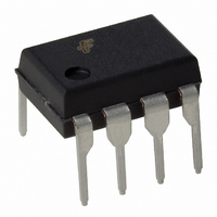
FSQ0370RNA Fairchild Semiconductor, FSQ0370RNA Datasheet - Page 4

FSQ0370RNA
Manufacturer Part Number
FSQ0370RNA
Description
IC SWIT PWM GREEN OVP UVLO 8DIP
Manufacturer
Fairchild Semiconductor
Series
FPS™r
Specifications of FSQ0370RNA
Output Isolation
Isolated
Frequency Range
92kHz ~ 108kHz
Voltage - Input
9 V ~ 20 V
Voltage - Output
700V
Power (watts)
27W
Operating Temperature
25°C ~ 140°C
Package / Case
8-DIP (0.300", 7.62mm)
Power Switch Family
FSQ0370
Power Switch On Resistance
4Ohm
Output Current
970mA
Number Of Outputs
Single
Mounting
Through Hole
Supply Current
3mA
Package Type
PDIP
Operating Temperature (min)
-25C
Operating Temperature (max)
85C
Operating Temperature Classification
Commercial
Pin Count
8
Power Dissipation
1.5W
On Resistance (max)
4 Ohms
Maximum Operating Temperature
+ 85 C
Minimum Operating Temperature
- 25 C
Maximum Power Dissipation
1500 mW
Mounting Style
Through Hole
Lead Free Status / RoHS Status
Lead free / RoHS Compliant
Available stocks
Company
Part Number
Manufacturer
Quantity
Price
Company:
Part Number:
FSQ0370RNA
Manufacturer:
FSC
Quantity:
81 000
Part Number:
FSQ0370RNA
Manufacturer:
FAIRCHILD/ن»™ç«¥
Quantity:
20 000
FSQ0170RNA, FSQ0270RNA, FSQ0370RNA Rev. 1.0.2
© 2006 Fairchild Semiconductor Corporation
Absolute Maximum Ratings
The “Absolute Maximum Ratings” are those values beyond which the safety of the device cannot be guaranteed. The
device should not be operated at these limits. The parametric values defined in the Electrical Characteristics tables
are not guaranteed at the absolute maximum ratings. T
Notes:
5. Non-repetitive rating: Pulse width is limited by maximum junction temperature.
6. L = 51mH, starting T
Thermal Impedance
T
Notes:
7. Free standing with no heatsink; without copper clad.
8. Measured on the DRAIN pin close to plastic interface.
9. Measured on the PKG top surface.
A
(Measurement Condition - Just before junction temperature T
= 25°C, unless otherwise specified. All items are tested with the standards JESD 51-2 and 51-10 (DIP).
Symbol
Symbol
V
V
T
DRAIN
E
V
V
I
θ
θ
θ
P
DM
T
T
STG
STR
CC
JA
JC
AS
FB
JT
A
D
J
Drain Pin Voltage
Vstr Pin Voltage
Drain Current Pulsed
Single Pulsed Avalanche Energy
Supply Voltage
Feedback Voltage Range
Total Power Dissipation
Operating Junction Temperature
Operating Ambient Temperature
Storage Temperature
Junction-to-Ambient Thermal Resistance
Junction-to-Case Thermal Resistance
Junction-to-Top Thermal Resistance
J
= 25°C.
Characteristic
(5)
Parameter
(6)
A
= 25°C, unless otherwise specified.
(9)
4
(8)
FSQ0170RNA
FSQ0270RNA
FSQ0370RNA
FSQ0170RNA
FSQ0270RNA
FSQ0370RNA
(7)
J
enters into OTP.)
Internally limited
-55 to +150
-0.3 to V
-25 to +85
Value
Value
700
700
140
230
1.5
80
20
35
12
50
20
4
8
CC
www.fairchildsemi.com
°C/W
°C/W
°C/W
Unit
Unit
mJ
°C
°C
°C
W
V
V
A
V
V


