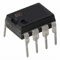
VIPER53EDIP-E STMicroelectronics, VIPER53EDIP-E Datasheet - Page 16

VIPER53EDIP-E
Manufacturer Part Number
VIPER53EDIP-E
Description
IC OFFLINE SWIT PWM CM OTP 8DIP
Manufacturer
STMicroelectronics
Series
VIPER™r
Datasheet
1.VIPER53ESPTR-E.pdf
(31 pages)
Specifications of VIPER53EDIP-E
Output Isolation
Isolated
Frequency Range
93 ~ 300kHz
Voltage - Input
8.4 ~ 19 V
Voltage - Output
620V
Power (watts)
30W
Operating Temperature
25°C ~ 125°C
Package / Case
8-DIP (0.300", 7.62mm)
For Use With
497-8435 - BOARD EVAL FOR VIPER53 28W497-6458 - BOARD EVAL BASED ON VIPER53-E497-6262 - BOARD REF SGL VIPER53 90-264VAC497-5866 - EVAL BOARD 24W NEG OUT VIPER53E497-5865 - EVAL BOARD 24W POS OUT VIPER53E497-4933 - BOARD PWR SUPPLY 24W OUTPUT VIPE
Lead Free Status / RoHS Status
Lead free / RoHS Compliant
Other names
497-6172-5
Available stocks
Company
Part Number
Manufacturer
Quantity
Price
Regulation Loop Stability
10
16/31
Regulation Loop Stability
The complete converter open loop transfer function can be built from both power cell and
the feedback network transfer functions. A theoretical example can be seen in
page 22
A typical schematic corresponding to this situation can be seen on
transfer function of the power cell is represented as G(s) in
a pole which depends on the output load and on the output capacitor value. As the load of a
converter may change, two curves are shown for two different values of output resistance
value, R
capacitor ESR. Note: The overall transfer function does not depend on the input voltage
because of the current mode control. A typical regulation loop is shown on
page 8
zero due to the R
and R
The total transfer function is shown as F(s). G(s) at the bottom of
maximum load (plain line), the load pole begins exactly where the zeros of the COMP pin
and the TL431 stop, and this results in a first order decreasing slope until it reaches the zero
of the output capacitor ESR. The point where the complete transfer function has a unity gain
is known as the regulation bandwidth and has a double interest:
In
ensured.
The dynamic load regulation is improved by increasing the regulation bandwidth, but some
limitations have to be respected:
1.
2.
As the highest bandwidth is obtained with the highest output power (Plain line with R
in
value of R
Go is the current transfer ratio of the optocoupler.
Figure
Figure 3 on page
– The higher it is, the faster the reaction will be to an eventual load change, and the
– The phase shift in the complete system at this point has to be less than 135° to
As the transfer function above zero due the ESR capacitor is not reliable (the ESR itself
is not well specified, and other parasitic effects may take place), the bandwidth should
always be lower than the minimum of FC and ESR zero
As the highest bandwidth is obtained with the highest output power (plain line with RL2
load in
value of R4 if R1 is set to a fixed value (e.g., (2.2k ).
2
smaller the output voltage change will be.
ensure good stability. Generally, a first-order slope gives 90° of phase shift, and a
second-order gives 180°.
-C
and has a fixed behavior represented by F(s) on
L1
for a discontinuous mode flyback loaded by a simple resistor.
2
3), the above criteria will be checked for this condition and allows to define the
4
and R
is set at the same value as the maximum load R
, if R1 is set fixed (2.2k , for instance). The following formula can be derived:
Figure
L2
1
-C
. A zero at higher frequency values then appears, due to the output
3, the above criteria will be checked for this condition and allows the
8, the unity gain is reached in a first order slope, so the stability is
1
network on the COMP pin and to the integrator built around the TL431
and:
with:
R
4
DocRev1
=
P
P
MAX
O UT2
-------------------- -
P
P
O UT2
MAX
=
=
1
-- - L
2
V
---------------- -
R L2
------------------------------------------------------- -
F
2
OUT
P
BW2
I
2
LIM
G
O
R
L2
F
R
SW
1
C
OUT
VIPer53EDIP - E / VIPer53ESP - E
Figure 11 on page
.Figure 11 on page 22
L2
pole.
Figure 11 on page
Figure 3 on page
Figure 3 on
22. A double
Figure 11 on
It exhibits
22. For
L2
8. The
load


