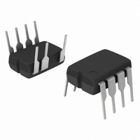
NCP1014AP065G ON Semiconductor, NCP1014AP065G Datasheet - Page 17

NCP1014AP065G
Manufacturer Part Number
NCP1014AP065G
Description
IC OFFLINE SWIT SMPS CM OVP 8DIP
Manufacturer
ON Semiconductor
Datasheet
1.NCP1010ST100T3G.pdf
(24 pages)
Specifications of NCP1014AP065G
Output Isolation
Isolated
Frequency Range
59 ~ 71kHz
Voltage - Input
8.5 ~ 10 V
Voltage - Output
700V
Power (watts)
19W
Operating Temperature
-40°C ~ 125°C
Package / Case
8-DIP (0.300", 7.62mm), 7 Leads
Duty Cycle (max)
72 %
Mounting Style
Through Hole
Switching Frequency
71 KHz
Operating Supply Voltage
- 0.3 V to + 10 V
Maximum Operating Temperature
+ 150 C
Synchronous Pin
No
Topology
Flyback
Lead Free Status / RoHS Status
Lead free / RoHS Compliant
Other names
NCP1014AP065GOS
Available stocks
Company
Part Number
Manufacturer
Quantity
Price
Company:
Part Number:
NCP1014AP065G
Manufacturer:
ON
Quantity:
5 000
Part Number:
NCP1014AP065G
Manufacturer:
ON/安森美
Quantity:
20 000
The Flyback transfer formula dictates that:
Ip and plugging into Equation 19, leads to:
Tsw = Lp
DCM operation is lost, there is another expression we can
write to connect Lp, the primary peak current bounded by
the NCP101X and the maximum duty- -cycle that needs to
stay below 50%:
corresponds to the lowest rectified bulk voltage, hence the
longest ton duration or largest duty- -cycle. Ip max is the
available peak current from the considered part, e.g. 350 mA
typical for the NCP1013 (however, the minimum value of
this parameter shall be considered for reliable evaluation).
Combining Equations 21 and 22 gives the maximum
theoretical power you can pass respecting the peak current
capability of the NCP101X, the maximum duty- -cycle and
the discontinuous mode operation:
current circulating in the MOSFET:
obtain the average dissipation in the MOSFET:
losses shall be added.
above calculations, we will discover that a power supply
built with the NCP101X and operating from a 100 Vac line
minimum will not be able to deliver more than 7.0 W
continuous, regardless of the selected switching frequency
(however the transformer core size will go down as
Fswitching
significantly when operated from a single European mains
(18 W). Application note AND8125/D, “Evaluating the
Power Capability of the NCP101X Members” details how
to assess the available power budget from all the NCP101X
series.
d =
Pavg = 1
(eq. 21)
Extracting Lp from Equation 20 gives:
If Lp critical gives the inductance value above which
From Equation 22 we obtain the operating duty- -cycle
If we stick to Equation 23, compute Lp and follow the
Pout
Lp critical =
Lpmax =
IdRMS = Ip ·
η =
Vin · Tsw
Ip · Lp
(2 · Lpmax · Vr 2 + 4 · Lpmax · Vr · Vinmin
3
, with Vr = N . (Vout + Vf) and η the efficiency.
1
2
· Ip 2 · d · R DSon
Pmax := Tsw 2 · Vinmin 2 · Vr 2 · η ·
DCmax · Vinmin · Tsw
· Lp · Ip 2 · Fsw
η · Fsw · Lp
is
2 · Fsw · [Pout · (Vr 2 + 2 · Vr · Vin + Vin 2 )]
2 · Pout
+ 2 · Lpmax · Vinmin 2 )
(eq. 24)
increased).
d
3
Ipmax
(eq. 25)
which lets us calculate the RMS
·
Fsw
Vin
(eq. 19)
1
(Vin · Vr) 2 · η
. From this equation, we
(eq. 26)
This
+
N · (Vout + Vf)
(eq. 22)
which, by extracting
number
to which switching
1
where Vinmin
increases
(eq. 20)
(eq. 23)
http://onsemi.com
17
Example 1. A 12 V 7.0 W SMPS operating on a large
mains with NCP101X:
Vin = 100 Vac to 250 Vac or 140 Vdc to 350 Vdc once
rectified, assuming a low bulk ripple
Efficiency = 80%
Vout = 12 V, Iout = 580 mA
Fswitching = 65 kHz
Ip max = 350 mA – 10% = 315 mA
Applying the above equations leads to:
Selected maximum reflected voltage = 120 V
with Vout = 12 V, secondary drop = 0.5 V Np:Ns = 1:0.1
Lp critical = 3.2 mH
Ip = 292 mA
Duty- -cycle worse case = 50%
Idrain RMS = 119 mA
P
P
Secondary diode voltage stress = (350 x 0.1) + 12 = 47 V
(e.g. a MBRS360T3, 3.0 A/60 V would fit)
Example 2. A 12 V 16 W SMPS operating on narrow
European mains with NCP101X:
Vin = 230 Vac 15%, 276 Vdc for Vin min to 370 Vdc
once rectified
Efficiency = 80%
Vout = 12 V, Iout = 1.25 A
Fswitching = 65 kHz
Ip max = 350 mA – 10% = 315 mA
Applying the equations leads to:
Selected maximum reflected voltage = 250 V
with Vout = 12 V, secondary drop = 0.5 V Np:Ns = 1:0.05
Lp = 6.6 mH
Ip = 0.305 mA
Duty- -cycle worse case = 0.47
Idrain RMS = 121 mA
P
P
ambient of 50C.
Secondary diode voltage stress = (370 x 0.05) + 12 = 30.5 V
(e.g. a MBRS340T3, 3.0 A/40 V)
whereas a 10 ms ripple naturally affects the final voltage
available on the transformer end. Once the Bulk capacitor has
been selected, one should check that the resulting ripple (min
Vbulk?) is still compatible with the above calculations. As an
example, to benefit from the largest operating range, a 7.0 W
board was built with a 47 mF bulk capacitor which ensured
discontinuous operation even in the ripple minimum waves.
MOSFET
DSS
MOSFET
DSS
Please note that these calculations assume a flat DC rail
= 1.1 mA x 370 V = 407 mW, if DSS is used below an
= 1.1 mA x 350 V = 385 mW, if DSS is used
= 354 mW at R
= 368 mW at R
DSon
DSon
= 24 Ω (T
= 24 Ω (T
J
J
> 100C)
> 100C)


