NCP1216P100G ON Semiconductor, NCP1216P100G Datasheet - Page 4
NCP1216P100G
Manufacturer Part Number
NCP1216P100G
Description
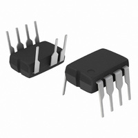
IC CTRLR PWM CM OTP HV 8DIP
Manufacturer
ON Semiconductor
Datasheet
1.NCP1216AP100G.pdf
(18 pages)
Specifications of NCP1216P100G
Output Isolation
Isolated
Frequency Range
90 ~ 110kHz
Voltage - Input
10 ~ 16 V
Operating Temperature
0°C ~ 150°C
Package / Case
8-DIP (0.300", 7.62mm), 7 Leads
Duty Cycle (max)
81 %
Mounting Style
Through Hole
Switching Frequency
110 KHz
Operating Supply Voltage
16 V
Maximum Operating Temperature
+ 150 C
Fall Time
20 ns
Rise Time
60 ns
Synchronous Pin
No
Topology
Flyback
Input Voltage
11V
Output Current
500mA
Frequency
100kHz
Supply Voltage Range
5.6V To 13.4V
Digital Ic Case Style
DIP
No. Of Pins
7
Operating Temperature Range
-25°C To +125°C
Rohs Compliant
Yes
Pwm Type
Current Mode PWM Controller
On/off Pin
No
Adjustable Output
Yes
Switching Freq
110kHz
Duty Cycle
81%
Operating Supply Voltage (max)
16V
Mounting
Through Hole
Pin Count
7
Package Type
PDIP
Lead Free Status / RoHS Status
Lead free / RoHS Compliant
Other names
NCP1216P100GOS
Available stocks
Company
Part Number
Manufacturer
Quantity
Price

Part Number:
NCP1216P100G
Manufacturer:
ON/安森美
Quantity:
20 000


1.
2. Maximum value at T
3. Minimum value for T
ELECTRICAL CHARACTERISTICS
V
DYNAMIC SELF−SUPPLY
INTERNAL STARTUP CURRENT SOURCE (T
DRIVE OUTPUT
CURRENT COMPARATOR (Pin 5 Unloaded)
V
V
V
Internal IC Consumption, No Output Load on Pin 5, F
Internal IC Consumption, No Output Load on Pin 5, F
Internal IC Consumption, No Output Load on Pin 5, F
Internal IC Consumption, 1.0 nF Output Load on Pin 5, F
Internal IC Consumption, 1.0 nF Output Load on Pin 5, F
Internal IC Consumption, 1.0 nF Output Load on Pin 5, F
Internal IC Consumption, Latchoff Phase, V
High−voltage Current Source, V
High−voltage Current Source, V
Output Voltage Rise−time @ C
Output Voltage Fall−time @ C
Source Resistance
Sink Resistance
Input Bias Current @ 1.0 V Input Level on Pin 3
Maximum Internal Current Setpoint
Default Internal Current Setpoint for Skip Cycle Operation
Propagation Delay from Current Detection to Gate OFF State
Leading Edge Blanking Duration
CC
CC
CC
CC
V
CC
= 11 V unless otherwise noted.)
Increasing Level at which the Current Source Turns Off
Decreasing Level at which the Current Source Turns On
Decreasing Level at which the Latchoff Phase Ends
OFF
and
V
CC
ON
J
J
min−max always ensure an hysteresis of 2.0 V.
= 0°C.
= 125°C.
L
L
= 1.0 nF, 10−90% of a 12 V Output Signal
Characteristic
CC
CC
= 1.0 nF, 10−90% of a 12 V Output Signal
= 10 V
= 0 V
(For typical values T
CC
J
= 6.0 V
> 0°C)
SW
SW
SW
= 65 kHz
= 100 kHz
= 133 kHz
SW
SW
SW
http://onsemi.com
= 65 kHz
= 100 kHz
= 133 kHz
J
= 25°C, for min/max values T
4
NCP1216A
NCP1216
Pin
6
6
6
6
6
6
6
6
6
6
8
8
5
5
5
5
3
3
3
3
3
VCC
VCC
Symbol
VCC
I
T
T
R
I
I
I
I
I
I
I
I
R
IC1
IC2
Lskip
CC1
CC1
CC1
CC2
CC2
CC2
CC3
Limit
I
DEL
LEB
J
T
T
OH
IB
OL
latch
r
f
OFF
= 0°C to +125°C, Maximum T
ON
(Note 3)
11.2
0.93
Min
9.2
4.9
5.0
15
1025
1060
12.2
10.0
0.02
1.08
Typ
990
250
320
330
220
5.6
1.7
2.1
2.4
8.0
9.0
60
20
20
10
80
(Note 1)
(Note 1)
(Note 2)
(Note 2)
(Note 2)
(Note 2)
(Note 2)
(Note 2)
1180
1200
1110
Max
13.4
11.0
1.14
J
130
2.0
2.4
2.9
35
18
11
= 150°C,
Unit
mA
mA
mA
mA
mA
mV
mA
mA
mA
mA
mA
ns
ns
ns
ns
V
V
V
W
W
V
Related parts for NCP1216P100G
Image
Part Number
Description
Manufacturer
Datasheet
Request
R

Part Number:
Description:
ON Semiconductor [VOLTAGE REGULATOR]
Manufacturer:
ON Semiconductor
Datasheet:
Part Number:
Description:
357-036-542-201 CARDEDGE 36POS DL .156 BLK LOPRO
Manufacturer:
ON Semiconductor
Datasheet:
Part Number:
Description:
357-036-542-201 CARDEDGE 36POS DL .156 BLK LOPRO
Manufacturer:
ON Semiconductor
Datasheet:
Part Number:
Description:
357-036-542-201 CARDEDGE 36POS DL .156 BLK LOPRO
Manufacturer:
ON Semiconductor
Datasheet:
Part Number:
Description:
357-036-542-201 CARDEDGE 36POS DL .156 BLK LOPRO
Manufacturer:
ON Semiconductor
Datasheet:
Part Number:
Description:
357-036-542-201 CARDEDGE 36POS DL .156 BLK LOPRO
Manufacturer:
ON Semiconductor
Datasheet:
Part Number:
Description:
357-036-542-201 CARDEDGE 36POS DL .156 BLK LOPRO
Manufacturer:
ON Semiconductor
Datasheet:
Part Number:
Description:
357-036-542-201 CARDEDGE 36POS DL .156 BLK LOPRO
Manufacturer:
ON Semiconductor
Datasheet:
Part Number:
Description:
357-036-542-201 CARDEDGE 36POS DL .156 BLK LOPRO
Manufacturer:
ON Semiconductor
Datasheet:
Part Number:
Description:
357-036-542-201 CARDEDGE 36POS DL .156 BLK LOPRO
Manufacturer:
ON Semiconductor
Datasheet:
Part Number:
Description:
357-036-542-201 CARDEDGE 36POS DL .156 BLK LOPRO
Manufacturer:
ON Semiconductor
Datasheet:
Part Number:
Description:
Manufacturer:
ON Semiconductor
Datasheet:
Part Number:
Description:
Manufacturer:
ON Semiconductor
Datasheet:
Part Number:
Description:
Manufacturer:
ON Semiconductor
Datasheet: