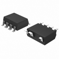
FSD200BM Fairchild Semiconductor, FSD200BM Datasheet - Page 9

FSD200BM
Manufacturer Part Number
FSD200BM
Description
IC SWIT PWM GREEN UVLO HV 7SOP
Manufacturer
Fairchild Semiconductor
Datasheet
1.FSD200BM.pdf
(18 pages)
Specifications of FSD200BM
Output Isolation
Isolated
Frequency Range
126 ~ 142kHz
Voltage - Input
6 ~ 10 V
Voltage - Output
670V
Power (watts)
7W
Operating Temperature
25°C ~ 100°C
Package / Case
8-SOP (7 Leads)
Power Switch Family
FSD200
Input Voltage
-0.3 to 10V
Power Switch On Resistance
28Ohm
Number Of Outputs
Single
Mounting
Surface Mount
Supply Current
600uA
Package Type
SOP
Operating Temperature (min)
-25C
Operating Temperature (max)
85C
Operating Temperature Classification
Commercial
Pin Count
7
Power Dissipation
1450W
Lead Free Status / RoHS Status
Lead free / RoHS Compliant
Other names
FSD200BM_NL
FSD200BM_NL
FSD200BM_NL
Available stocks
Company
Part Number
Manufacturer
Quantity
Price
Company:
Part Number:
FSD200BM/FSD200M
Manufacturer:
FAI
Quantity:
1 950
Company:
Part Number:
FSD200BMX
Manufacturer:
FSC
Quantity:
2 000
Company:
Part Number:
FSD200BMX
Manufacturer:
EUDYNA
Quantity:
100
Functional Description
1. Startup : At startup, the internal high voltage current
source supplies the internal bias and charges the external
Vcc capacitor as shown in Figure 7. In the case of the
FSD210B, when Vcc reaches 8.7V the device starts
switching and the internal high voltage current source is
disabled. The device is in normal operation provided that
Vcc does not drop below 6.7V. After startup the bias is
supplied from the auxiliary transformer winding. In the case
of FSD200B, An internal high voltage regulator (HV Req.)
located between Vstr pin and Vcc pin regulates the Vcc to be
7V and supplies operating current, thus FSD200B needs no
auxiliary bias winding.
V
V
Vin,dc
Vcc
START
STOP
Figure 7. Charging Vcc Capacitor through Vstr
Vcc
Figure 6. Internal Startup Circuit
I
VCC
I
UVLO
8.7V/
6.7V
VCC
= I
Vin,dc
STR
= I
STR
-I
L
START
Vcc
-I
H
FSD210B
START
I
STR
Vstr
I
START
Vcc must not drop
Bias winding
Vin,dc
below V
UVLO
voltage
Vref
I
STR
Vcc
STOP
Vstr
J-FET
FSD2xx
7V
I
STR
Reg.
HV
FSD200B
t
Vstr
Calculating the Vcc capacitor is an important step to design
with the FSD200B/210B. At initial start-up in the both
devices, the maximum value of start operating current
I
and Vref Blocks. The charging current I
capacitor is equal to I
UVLO start voltage only the bias winding supplies Vcc
current to device. When the bias winding voltage is not suffi-
cient, the Vcc level decreases to the UVLO stop voltage. At
this time Vcc oscillates. In order to prevent this oscillation it
is recommended that the Vcc capacitor be chosen to have the
value between 10uF and 47uF.
2. Feedback Control : The FSD200B/210B are voltage
mode controlled devices as shown in Figure 8. Usually, an
opto-coupler and KA431 type voltage reference are used to
implement the feedback network. The feedback voltage is
compared with an internally generated sawtooth waveform.
This directly controls the duty cycle. When the KA431
reference pin voltage exceeds the internal reference voltage
of 2.5V, the optocoupler LED current increases, the feedback
voltage Vfb is pulled down and it reduces the duty cycle.
This will happen when the input voltage increases or the
output load decreases.
3. Leading Edge Blanking (LEB) : At the instant the inter-
nal Sense FET is turned on, the primary side capacitance and
secondary side rectifier diode reverse recovery typically
cause a high current spike through the Sense FET. Excessive
voltage across the Rsense resistor leads to incorrect feedback
operation in the current mode PWM control. To counter this
effect, the FPS employs a leading edge blanking (LEB) cir-
cuit. This circuit inhibits the PWM comparator for a short
time (t
START
Vo
LEB
is about 100uA, which supplies current to UVLO
KA431
) after the Sense FET is turned on.
Figure 8. PWM and Feedback Circuit
Vfb
Cfb
4
V
STR
+
5uA
-
FB
V
Vcc
SD
- 100uA. After Vcc reaches the
Vref
0.25mA
R
OSC
OLP
FSD210B, FSD200B
Vcc
driver
Gate
of the Vcc
9


