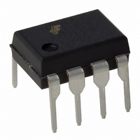
FSDL321 Fairchild Semiconductor, FSDL321 Datasheet - Page 12

FSDL321
Manufacturer Part Number
FSDL321
Description
IC SWIT PWM GREEN CM OVP HV 8DIP
Manufacturer
Fairchild Semiconductor
Specifications of FSDL321
Output Isolation
Isolated
Frequency Range
45 ~ 55kHz
Voltage - Input
8 ~ 20 V
Voltage - Output
650V
Power (watts)
17W
Operating Temperature
25°C ~ 140°C
Package / Case
8-DIP (0.300", 7.62mm)
Power Switch Family
FSDL321
Power Switch On Resistance
14Ohm
Output Current
2A
Number Of Outputs
Single
Mounting
Through Hole
Supply Current
3mA
Package Type
PDIP
Operating Temperature (min)
-25C
Operating Temperature (max)
85C
Operating Temperature Classification
Commercial
Pin Count
8
Power Dissipation
1.4W
Lead Free Status / RoHS Status
Lead free / RoHS Compliant
Other names
FSDL321_NL
FSDL321_NL
FSDL321_NL
FSDH321, FSDL321
6. Burst operation :In order to minimize power dissipation
in standby mode, the FPS
As the load decreases, the feedback voltage decreases. As
shown in figure 10, the device automatically enters burst
mode when the feedback voltage drops below
V
limit is set to a fixed limit internally to minimize flux density
in the transformer. The fixed current limit is larger than that
defined by Vfb = V
further. Switching continues until the feedback voltage drops
below V
the output voltages start to drop at a rate dependent on the
standby current load. This causes the feedback voltage to
rise. Once it passes V
The feedback voltage then falls and the process repeats.
Burst mode operation alternately enables and disables
switching of the power Sense FET thereby reducing switch-
ing loss in Standby mode.
12
FB
BURH
3
(500mV). Switching still continues but the current
0.35V/0.5V
BURL
I
delay
0.3/0.5V
S W IT C H
Vcc
0.5V
O F F
0.5V
Figure 8. Soft Start Function
Figure 9. Circuit for Burst operation
(350mV). At this point switching stops and
Vcc
+
-
BURH
I
FB
BURH
5 V
TM
2.5R
and therefore, Vfb is driven down
I_ o v e r
(500mV) switching resumes.
enters burst mode operation.
R
Normal
R s e n s e
Burst
D R A I N
G N D
Vcc
I
B_PEAK
MOSFET
Current
PWM
7. Frequency Modulation : EMI reduction can be accom-
plished by modulating the switching frequency of a switched
power supply. Frequency modulation can reduce EMI by
spreading the energy over a wider frequency range than the
band width measured by the EMI test equipment. The
amount of EMI reduction is directly related to the depth of
the reference frequency. As can be seen in Figure 11, the fre-
quency changes from 97KHz to 100KHz (from 48.5KHz to
51.5KHz for FSDL321)in 4mS for the FSDH321. Frequency
modulation allows the use of a cost effective inductor instead
of an AC input mode choke to satisfy the requirements of
world wide EMI limits.
Figure 11. Frequency Modulation Waveform for FSDH321
waveform
0.5V
0.3V
Current
0.5V
0.35V
Feedback
Figure 10. Circuit for Burst Operation
Drain to
Drain to
Drain to
Drain to
Burst Operation
Source
Source
voltage
voltage
Switching OFF
Turn-on
Turn-on
Oscillator
Oscillator
Internal
Internal
Waveform
Waveform
97kHz
97kHz
Vds
Vds
103kHz
103kHz
100kHz
100kHz
103kHz
103kHz
Burst Operation
Switching OFF
Turn-off
Turn-off
6kHz
6kHz
Normal Operation


