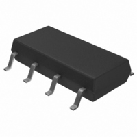
FSDM0365RL Fairchild Semiconductor, FSDM0365RL Datasheet

FSDM0365RL
Specifications of FSDM0365RL
FSDM0365RL_NL
Available stocks
Related parts for FSDM0365RL
FSDM0365RL Summary of contents
Page 1
... FSDH0265RL 16W 27W FSDL0365RL 19W 30W FSDM0365RL 19W 30W Table 1. Notes: 1. Typical continuous power in a non-ven- tilated enclosed adapter with sufficient drain pattern or something as a heat sinker measured at 50°C ambient. 2. Maximum practical continuous power in an open frame design with sufficient drain pattern or something as a heat sinker at 50° ...
Page 2
FSDL0365RN, FSDM0365RN Internal Block Diagram + V /V BURL BURH - V BURH Vcc Vcc I I delay 2. Vcc Vovp TSD 2 Vcc 2 8V/12V Vcc good Vcc Freq. Modulation ...
Page 3
Pin Definitions Pin Number Pin Name 1 GND 2 Vcc 3 Vfb 4 Ipk 5 Vstr Drain Pin Configuration Pin Function Description Sense FET source terminal on primary side and internal control ground. Positive supply voltage input. ...
Page 4
FSDL0365RN, FSDM0365RN Absolute Maximum Ratings (Ta=25°C, unless otherwise specified) Characteristic Maximum Drain Pin Voltage Maximum Vstr Pin Voltage (1) Drain Current Pulsed Single Pulsed Avalanche Energy Maximum Supply Voltage Analog Input Voltage Range Total Power Dissipation Operating Junction Temperature. Operating ...
Page 5
Electrical Characteristics (Ta = 25°C unless otherwise specified) Parameter Sense FET SECTION Off-State Current (Max.Rating =660V) On-State Resistance (1) Input Capacitance Output Capacitance Reverse Transfer Capacitance Turn On Delay Time Rise Time Turn Off Delay Time Fall Time CONTROL SECTION ...
Page 6
FSDL0365RN, FSDM0365RN Shutdown Feedback Voltage Over Voltage Protection Shutdown Feedback Delay Current Leading Edge Blanking Time TOTAL DEVICE SECTION Operating Current Start Up Current Vstr Supply Voltage Note: ≤ 1. Pulse test: Pulse width 300uS, duty 2. These parameters, although ...
Page 7
Comparison Between KA5x0365RN and FSDx0365RN Function KA5x0365RN Soft-Start not applicable External Current Limit not applicable Frequency Modulation not applicable Burst Mode Operation not applicable Drain Creepage at 1,02mm Package FSDx0365RN FSDx0365RN Advantages 15mS • Gradually increasing current limit during soft-start ...
Page 8
FSDL0365RN, FSDM0365RN Typical Performance Characteristics (Sense FET part) 8.0 7.5 7.0 6.5 6.0 5 5.0 4.5 4.0 3.5 3.0 2 Drain Current [A] D On-Resistance vs. Drain Current 700 600 C 500 ...
Page 9
Typical Performance Characteristics 1.15 1.10 1.05 1.00 0.95 0.90 - Junction Temperature [ J Breakdown Voltage vs. Temperature 1 Operation in This Area 10 is Limited by R DS(on ...
Page 10
FSDL0365RN, FSDM0365RN Typical Performance Characteristics (Control Part) (These characteristic graphs are normalized 1.20 1.00 0.80 0.60 0.40 0.20 0.00 - emp[ ℃ ] Operating Frequency (Fosc) 1.20 1.00 0.80 0.60 0.40 0.20 0.00 -50 ...
Page 11
Typical Performance Characteristics 1.20 1.00 0.80 0.60 0.40 0.20 0.00 - emp[ ℃ ] Feedback Source Current (Ifb) 1.20 1.00 0.80 0.60 0.40 0.20 0.00 - emp[ ℃ ] Start up Current (Istart) 1.20 1.00 0.80 ...
Page 12
FSDL0365RN, FSDM0365RN Functional Description 1. Startup : In previous generations of Fairchild Power Switches (FPS) the Vstr pin had an external resistor to the DC input voltage line. In this generation the startup resistor is replaced by an internal high ...
Page 13
Vcc 8V OLP 6V FPS switching 3V Delay current (5uA) charges the Cfb − − ...
Page 14
FSDL0365RN, FSDM0365RN Figure 8. Soft Start Function 6. Burst operation : In order to minimize power standby mode, the FPS enters burst mode V / ...
Page 15
Frequency (MHz) Figure 12. KA5-series FPS Full Range EMI scan(67KHz, no Frequency Modulation) with DVD Player SET Frequency (MHz) Figure 13. FSDX-series FPS Full Range EMI Scan (67KHz, with Frequency Modulation) with DVD Player SET 8. Adjusting Current limit function: ...
Page 16
FSDL0365RN, FSDM0365RN Typical application circuit 1. Set Top Box Example Circuit (20W Output Power) 2A/250V FUSE 85VAC 100pF LF1 ~275VAC /400V KBP06M 40mH C1 100pF /400V C2 GreenFPS PERFORMANCE SUMMARY Output Power: 20W Regulation 3.3V: ±5% 5.0V: ±5% 17.0V: ±7% ...
Page 17
Transformer Specification SFO SPEC IFIC ATIO N - SCHEM ATIC DIAG R AM (TR ANSFO RM ER INDIN G SPEC IFIC ATIO N NO. PIN(S → ...
Page 18
FSDL0365RN, FSDM0365RN Layout Considerations DC_link Capacitor #1 : GND #2 : VCC #3 : Vfb #4 : Ipk #5 : Vstr #6 : Drain #7 : Drain #8 : Drain Figure 15. Layout Considerations for FSDx0365RN using 8DIP 18 SURFACE ...
Page 19
Package Dimensions 8DIP FSDL0365RN, FSDM0365RN 19 ...
Page 20
FSDL0365RN, FSDM0365RN Package Dimensions 20 (Continued) 8LSOP ...
Page 21
... Ordering Information Product Number Package FSDM0365RN 8DIP FSDL0365RN 8DIP FSDM0365RL 8LSOP FSDL0365RL 8LSOP Marking Code BV DSS DM0365R 650V DL0365R 650V DM0365R 650V DL0365R 650V FSDL0365RN, FSDM0365RN F R OSC DS(on) 67KHz 3.6Ω 50KHz 3.6Ω 67KHz 3.6Ω 50KHz 3.6Ω ...
Page 22
... FSDL0365RN, FSDM0365RN DISCLAIMER FAIRCHILD SEMICONDUCTOR RESERVES THE RIGHT TO MAKE CHANGES WITHOUT FURTHER NOTICE TO ANY PRODUCTS HEREIN TO IMPROVE RELIABILITY, FUNCTION OR DESIGN. FAIRCHILD DOES NOT ASSUME ANY LIABILITY ARISING OUT OF THE APPLICATION OR USE OF ANY PRODUCT OR CIRCUIT DESCRIBED HEREIN; NEITHER DOES IT CONVEY ANY LICENSE UNDER ITS PATENT RIGHTS, NOR THE RIGHTS OF OTHERS. ...


