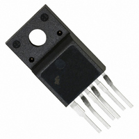
FSDM07652RWDTU Fairchild Semiconductor, FSDM07652RWDTU Datasheet - Page 12

FSDM07652RWDTU
Manufacturer Part Number
FSDM07652RWDTU
Description
IC SWIT PWM GREEN CM HV TO220F
Manufacturer
Fairchild Semiconductor
Datasheet
1.FSDM07652RWDTU.pdf
(20 pages)
Specifications of FSDM07652RWDTU
Output Isolation
Isolated
Frequency Range
60 ~ 72kHz
Voltage - Input
8 ~ 20 V
Voltage - Output
650V
Power (watts)
80W
Operating Temperature
25°C ~ 150°C
Package / Case
TO-220-6 Full Pack Formed Leads
Lead Free Status / RoHS Status
Lead free / RoHS Compliant
Other names
FSDM07652RWDTU_NL
FSDM07652RWDTU_NL
FSDM07652RWDTU_NL
FSDM07652R
3.1 Over Load Protection (OLP) : Overload is defined as
the load current exceeding a pre-set level due to an
unexpected event. In this situation, the protection circuit
should be activated in order to protect the SMPS. However,
even when the SMPS is in the normal operation, the over
load protection circuit can be activated during the load
transition. In order to avoid this undesired operation, the over
load protection circuit is designed to be activated after a
specified time to determine whether it is a transient situation
or an overload situation. Because of the pulse-by-pulse
current limit capability, the maximum peak current through
the Sense FET is limited, and therefore the maximum input
power is restricted with a given input voltage. If the output
consumes beyond this maximum power, the output voltage
(Vo) decreases below the set voltage. This reduces the
current through the opto-coupler LED, which also reduces
the opto-coupler transistor current, thus increasing the
feedback voltage (Vfb). If Vfb exceeds 2.5V, D1 is blocked
and the 3.5uA current source starts to charge C
Vcc. In this condition, Vfb continues increasing until it
reaches 6V, when the switching operation is terminated as
shown in figure 7. The delay time for shutdown is the time
required to charge C
general, a 10 ~ 50 ms delay time is typical for most
applications.
12
Vds
Vcc
12V
8V
Power
on
Figure 6. Auto restart operation
operation
Normal
B
from 2.5V to 6.0V with 3.5uA. In
occurs
Fault
situation
Fault
removed
Fault
operation
B
Normal
slowly up to
t
AOCP (Abnormal Over Current Protection) circuit as shown
in figure 8. When the gate turn-on signal is applied to the
power Sense FET, the AOCP block is enabled and monitors
the current through the sensing resistor. The voltage across
the resistor is then compared with a preset AOCP level. If the
sensing resistor voltage is greater than the AOCP level for
longer than 300ns, the reset signal is applied to the latch,
resulting in the shutdown of SMPS.
3.2 Abnormal Over Current Protection (AOCP) : Even
though the FPS
current mode PWM feedback, these are not enough to protect
the FPS
transformer pin short occurs. The FPS
3.3 Over voltage Protection (OVP) : If the secondary side
feedback circuit were to malfunction or a solder defect
caused an open in the feedback path, the current through the
opto-coupler transistor becomes almost zero. Then, Vfb
climbs up in a similar manner to the over load situation,
forcing the preset maximum current to be supplied to the
SMPS until the over load protection is activated. Because
more energy than required is provided to the output, the
6.0V
6.0V
6.0V
6.0V
2.5V
2.5V
2.5V
2.5V
V V V V
FB
FB
FB
FB
2.5R
R
TM
AOCP
when a secondary side diode short or a
Figure 7. Over load protection
OSC
T T T T
TM
1 1 1 1
PWM
Figure 8. AOCP block
has OLP (Over Load Protection) and
LEB
T T T T
Over load protection
Over load protection
Over load protection
Over load protection
S
R
12
12
12
12
= Cfb*(6.0-2.5)/I
= Cfb*(6.0-2.5)/I
= Cfb*(6.0-2.5)/I
= Cfb*(6.0-2.5)/I
Q
Q
+
-
Vaocp
driver
Gate
TM
delay
delay
delay
delay
R
has an internal
sense
T T T T
2 2 2 2
2
GND
t t t t


