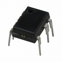
FSD200 Fairchild Semiconductor, FSD200 Datasheet - Page 10

FSD200
Manufacturer Part Number
FSD200
Description
IC SWIT PWM GREEN UVLO HV 7DIP
Manufacturer
Fairchild Semiconductor
Datasheet
1.FSD210.pdf
(18 pages)
Specifications of FSD200
Output Isolation
Isolated
Frequency Range
126 ~ 142kHz
Voltage - Input
6 ~ 10 V
Voltage - Output
700V
Power (watts)
7W
Operating Temperature
25°C ~ 100°C
Package / Case
8-DIP (0.300", 7.62mm), 7 Leads
Lead Free Status / RoHS Status
Lead free / RoHS Compliant
Other names
FSD200_NL
FSD200_NL
FSD200_NL
Available stocks
Company
Part Number
Manufacturer
Quantity
Price
Company:
Part Number:
FSD200
Manufacturer:
FAIRCHILD
Quantity:
10 000
Part Number:
FSD200
Manufacturer:
FAIRCHILD/ن»™ç«¥
Quantity:
20 000
Part Number:
FSD200B
Manufacturer:
FAIRCHILD/ن»™ç«¥
Quantity:
20 000
Company:
Part Number:
FSD200BM/M
Manufacturer:
FAI
Quantity:
1 950
Company:
Part Number:
FSD200BMX
Manufacturer:
FSC
Quantity:
2 000
Company:
Part Number:
FSD200BMX
Manufacturer:
EUDYNA
Quantity:
100
Part Number:
FSD200M
Manufacturer:
FAIRCHILD/ن»™ç«¥
Quantity:
20 000
FSD210, FSD200
reliability is improved without a cost increase. If either of
these thresholds are triggered, the FPS starts an auto-restart
cycle. Once the fault condition occurs, switching is termi-
nated and the Sense FET remains off. This causes Vcc to
fall. When Vcc reaches the UVLO stop voltage
(6.7V:FSD210, 6V:FSD200), the protection is reset and the
internal high voltage current source charges the Vcc capaci-
tor. When Vcc reaches the UVLO start voltage
(8.7V:FSD210,7V:FSD200), the device attempts to resume
normal operation. If the fault condition is no longer present
start up will be successful. If it is still present the cycle is
repeated (see figure 10).
4.1 Over Load Protection (OLP) : Over load protection
occurs when the load current exceeds a pre-set level due to
an abnormal situation. If this occurs, the protection circuit
should be triggered to protect the SMPS. It is possible that a
short term load transient can occur under normal operation.
In order to avoid false shutdowns, the over load protection
circuit is designed to trigger after a delay. Therefore the
device can differentiate between transient over loads and
true fault conditions. The maximum input power is limited
using the pulse-by-pulse current limit feature. If the load
tries to
draw more than this, the output voltage will drop below its
set value. This reduces the optocoupler LED current which
in turn reduces the photo-transistor current (see figure 9).
Therefore, the 250uA current source will charge the feed-
back pin capacitor, Cfb, and the feedback voltage, Vfb, will
increase. The input to the feedback comparator is clamped at
3V. Once Vfb reaches 3V, the device switches at maximum
power, the 250uA current source is blocked and the 5uA
source continues to charge Cfb. Once Vfb reaches 4V,
switching stops.and overload protection is triggered. The
resultant shutdown delay time is set by the time required to
charge Cfb from 3Vto 4Vwith 5uA as shown in Fig. 10.
4.2 Thermal Shutdown (TSD) : The Sense FET and the
control IC are integrated, making it easier for the control IC
10
Cfb
Vfb
4
Figure 9. Protection block
5uA
RESET
250uA
R
Vth 4V
3V
OLP
+
-
OSC
TSD
A/R
S
R
S
R
Q
Q
Protection Block
OLP, TSD
FSD2xx
DRIVER
GATE
to detect the temperature of the Sense FET. When the tem-
perature exceeds approximately 145°C, thermal shutdown is
activated.
5. Soft Start : FSD200/210 has an internal soft start circuit
that gradually increases current through the Sense FET as
shown in figure 11. The soft start time is 3msec in FSD200/
210.
6. Burst operation : In order to minimize the power dissipa-
tion in standby mode, the FSD200/210 implements burst
mode functionality (see figure 12). As the load decreases, the
feedback voltage decreases. As shown in figure 13, the
device automatically enters burst mode when the feedback
voltage drops below V
stops and the output voltages start to drop at a rate dependant
on standby current load. This causes the feedback voltage to
rise. Once it passes V
The feedback voltage falls and the process repeats. Burst
mode operation alternately enables and disables switching of
the power Sense FET thereby reducing switching loss in
I(A)
OLP
Vfb
4V
3V
t1<<t2, t3
t1 = -1/RC Χ Χ Χ Χ ln( 1-v(t1)/R )
t2 = Cfb Χ Χ Χ Χ {v(t1+t2)-v(t1)} / / / / Idelay
t1
0.2A
Figure 10. Over load protection delay
Figure 11. Internal Soft Start
t2
3mS
FPS Switching Area
Idelay (5uA) charges Cfb
BURH
BURL
FSD200/210
0.25A
(0.64V) switching starts again.
(0.58V). At this point switching
t3
v(t1)=3V
under Vstop of UVLO
0.3A
IC Reset
Iover
t
t


