FS6X1220RJ Fairchild Semiconductor, FS6X1220RJ Datasheet - Page 3
FS6X1220RJ
Manufacturer Part Number
FS6X1220RJ
Description
IC SWIT PWM CM OVP UVLO HV D2PAK
Manufacturer
Fairchild Semiconductor
Datasheet
1.FS6X0420RJ.pdf
(15 pages)
Specifications of FS6X1220RJ
Output Isolation
Isolated
Frequency Range
270 ~ 330kHz
Voltage - Input
9 ~ 35 V
Voltage - Output
200V
Power (watts)
36W
Operating Temperature
-25°C ~ 150°C
Package / Case
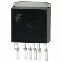
TO-263-7, D²Pak (6 leads + Tab), TO-263CB
Number Of Outputs
1
Duty Cycle (max)
88 %
Mounting Style
SMD/SMT
Switching Frequency
300 KHz
Operating Supply Voltage
35 V
Maximum Operating Temperature
+ 85 C
Minimum Operating Temperature
- 25 C
Synchronous Pin
No
Topology
Flyback, Forward
Lead Free Status / RoHS Status
Lead free / RoHS Compliant
Available stocks
Company
Part Number
Manufacturer
Quantity
Price
Company:

Part Number:
FS6X1220RJX
Manufacturer:
Fairchild Semiconductor
Quantity:
135


FS6X0420RJ/ FS6X0720RJ/ FS6X1220RJ Rev. 1.0.1
Pin Assignments
Pin Definitions
Pin Number
1
2
3
4
5
6
Line Sense (LS)
Pin Name
Feedback
Drain
GND
(FB)
N.C.
Vcc
Figure 3. Pin Configuration (Top View)
This pin is the high voltage power SenseFET drain connection.
This pin is the control ground and the SenseFET source.
This pin is the positive supply input. This pin provides internal operating current for both
start-up and steady-state operation.
This pin is internally connected to the inverting input of the PWM comparator. The collec-
tor of an opto-coupler is typically tied to this pin. For stable operation, a capacitor should
be placed between this pin and GND. If the voltage of this pin reaches 7.5V, the over load
protection is activated resulting in shutdown of the IC.
This pin is not connected.
According to the voltage of this pin, three operation modes are defined: normal operation
mode, line under voltage lock out mode, and sleep mode. If the voltage of this pin is
smaller than 2.55V, the IC goes into the line under voltage lock out, stopping switching
operation. If the voltage of this pin is smaller than 1.8V, the IC enters into sleep mode.
During sleep mode, reference voltage generation circuit including the shunt regulator is
disabled and only 300uA operation current is required.
D2-PAK-6L
3
6. Line Sense
5. N.C.
4. Vfb
3. Vcc
2. GND
1. Drain
Pin Function Description
www.fairchildsemi.com
Related parts for FS6X1220RJ
Image
Part Number
Description
Manufacturer
Datasheet
Request
R

Part Number:
Description:
Fairchild Semiconductor [IGBT MODULE]
Manufacturer:
Fairchild Semiconductor
Datasheet:

Part Number:
Description:
Discrete Semiconductor Modules
Manufacturer:
Fairchild Semiconductor
Part Number:
Description:
Discrete Semiconductor Modules
Manufacturer:
Fairchild Semiconductor
Part Number:
Description:
This N-Channel MOSFET is produced using Fairchild Semiconductor’s advanced Power Trench® process
Manufacturer:
Fairchild Semiconductor
Datasheet:
Part Number:
Description:
This N-Channel MOSFET is produced using Fairchild Semiconductor’s advanced Power Trench® process
Manufacturer:
Fairchild Semiconductor
Datasheet:
Part Number:
Description:
This N-Channel MOSFET is produced using Fairchild Semiconductor’s advanced PowerTrench® process
Manufacturer:
Fairchild Semiconductor
Datasheet:
Part Number:
Description:
This N-Channel MOSFET is produced using Fairchild Semiconductor’s advanced PowerTrench® process
Manufacturer:
Fairchild Semiconductor
Datasheet:
Part Number:
Description:
This N-Channel MOSFET is produced using Fairchild Semiconductor’s advanced Power Trench® process
Manufacturer:
Fairchild Semiconductor
Datasheet:
Part Number:
Description:
This N-Channel logic Level MOSFETs are produced using Fairchild Semiconductor‘s advanced Power Trench® process that has been special tailored to minimize the on-state resistance and yet maintain superior switching performance
Manufacturer:
Fairchild Semiconductor
Datasheet:
Part Number:
Description:
This N-Channel MOSFET is produced using Fairchild Semiconductor’s advanced Power Trench® process
Manufacturer:
Fairchild Semiconductor
Datasheet:
Part Number:
Description:
This N-Channel SyncFET™ is produced using Fairchild Semiconductor’s advanced PowerTrench® process
Manufacturer:
Fairchild Semiconductor
Datasheet:
Part Number:
Description:
This N-Channel SyncFET™ is produced using Fairchild Semiconductor’s advanced PowerTrench® process
Manufacturer:
Fairchild Semiconductor
Datasheet:
Part Number:
Description:
This N-Channel SyncFET™ is produced using Fairchild Semiconductor’s advanced PowerTrench® process
Manufacturer:
Fairchild Semiconductor
Datasheet:
Part Number:
Description:
This N-Channel logic Level MOSFETs are produced using Fairchild Semiconductor‘s advanced Power Trench® process that has been special tailored to minimize the on-state resistance and yet maintain superior switching performance
Manufacturer:
Fairchild Semiconductor
Datasheet:
Part Number:
Description:
This N-Channel MOSFET is produced using Fairchild Semiconductor’s advanced Power Trench® process that has been especially tailored to minimize the on-state resistance and yet maintain superior switching performance
Manufacturer:
Fairchild Semiconductor
Datasheet: