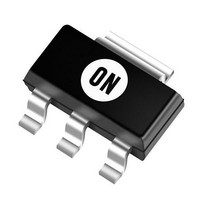
NCP1011ST100T3 ON Semiconductor, NCP1011ST100T3 Datasheet - Page 3

NCP1011ST100T3
Manufacturer Part Number
NCP1011ST100T3
Description
IC OFFLINE SWIT SMPS CM SOT223
Manufacturer
ON Semiconductor
Type
Self-Supplied Monolithic Switcherr
Datasheet
1.NCP1010ST100T3G.pdf
(24 pages)
Specifications of NCP1011ST100T3
Output Isolation
Isolated
Frequency Range
90 ~ 110kHz
Voltage - Input
8.5 ~ 10 V
Voltage - Output
700V
Power (watts)
19W
Operating Temperature
-40°C ~ 125°C
Package / Case
TO-261-4, TO-261AA, SOT-223-4
Input Voltage Range
- 0.3 V to + 10 V
Mounting Style
SMD/SMT
Lead Free Status / RoHS Status
Contains lead / RoHS non-compliant
GND
V
PIN FUNCTION DESCRIPTION
(SOT- -223)
NC
FB
CC
Pin No.
1
--
--
2
3
--
--
4
1
2
3
4
*Vclamp = VCC
Vclamp*
IV
CC
4 V
18 k
PDIP- -7/Gull Wing)
I?
(PDIP- -7,
V
Pin No.
CC
OFF
1
2
3
4
5
--
7
8
Error flag armed?
+ 200 mV (8.7 V Typical)
Startup Source
Management
EMI Jittering
UVLO
Pin Name
Overload?
Figure 2. Simplified Internal Circuit Architecture
Drain
GND
GND
GND
V
NC
FB
CC
--
High when V
Drain
Powers the Internal Circuitry
Feedback Signal Input
Drain Connection
65, 100 or
http://onsemi.com
Iref = 7.4 mA
130 kHz
The IC Ground
The IC Ground
The IC Ground
Clock
Function
CC
0.5 V
IV
Soft--Start
< 3 V
CC
--
--
3
+
--
Set
+
--
DCmax = 65%
Startup Sequence
Overload
R
Flip--Flop
Reset
Reset
S
Q
This pin is connected to an external capacitor of typic-
ally 10 mF. The natural ripple superimposed on the
V
proved standby performance, an auxiliary V
connected to Pin 1. The V
shunt which serves as an opto fail--safe protection.
By connecting an optocoupler to this pin, the peak
current setpoint is adjusted accordingly to the output
power demand.
The internal drain MOSFET connection.
CC
participates to the frequency jittering. For im-
Q
Driver
V
--
+
CC
Description
250 ns
L.E.B.
CC
--
--
--
--
--
also includes an active
Rsense
Drain
CC
8
7
5
can be
Drain
GND
GND


