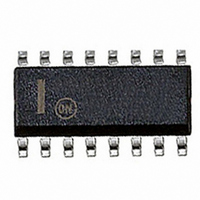
NCP1205DR2G ON Semiconductor, NCP1205DR2G Datasheet - Page 7

NCP1205DR2G
Manufacturer Part Number
NCP1205DR2G
Description
IC CTRLR PWM CM OVP HV 16SOIC
Manufacturer
ON Semiconductor
Datasheet
1.NCP1205DR2.pdf
(17 pages)
Specifications of NCP1205DR2G
Output Isolation
Isolated
Frequency Range
90 ~ 125kHz
Voltage - Input
8 ~ 30 V
Operating Temperature
-25°C ~ 150°C
Package / Case
16-SOIC (0.154", 3.90mm Width)
Number Of Outputs
1
Output Current
250 mA
Mounting Style
SMD/SMT
Switching Frequency
110 KHz
Operating Supply Voltage
30 V
Maximum Operating Temperature
+ 125 C
Fall Time
30 ns
Minimum Operating Temperature
- 25 C
Rise Time
30 ns
Synchronous Pin
No
Topology
Flyback, Forward
Lead Free Status / RoHS Status
Lead free / RoHS Compliant
Other names
NCP1205DR2G
NCP1205DR2GOSTR
NCP1205DR2GOSTR
Available stocks
Company
Part Number
Manufacturer
Quantity
Price
Part Number:
NCP1205DR2G
Manufacturer:
ON/安森美
Quantity:
20 000
4. Typical capacitor swing is between 0.5 V and 3.5 V.
5. Guaranteed by design, T
ELECTRICAL CHARACTERISTICS (continued)
Max T
Current Sense Comparator (continued)
Frequency Modulator
Drive Output
Undervoltage Lockout
Startup Current Source
Device Current Consumption
Propagation Delay from Current Detection to Gate OFF
Leading Edge Blanking (LEB)
Minimum Frequency Operation @ Ct = 1.0 F and
Maximum Frequency Operation @ Ct = 1.0 F and
Minimum Ct Charging Current (Note 4)
Maximum Ct Charging Current (Note 4)
Discharge Time @ Ct = 1.0 F
Output Voltage Rise Time @ C
Output Voltage Fall Time @ C
Clamped Output Voltage @ V
Voltage Drop on the Stage @ V
Startup Threshold (V
Minimum Operating Voltage (V
Maximum Voltage, Pin 1 Grounded
Maximum Voltage, Pin 1 Decoupled (470 mF)
Startup Current Source Flowing through Pin 1
Leakage Current in Offstate @ Vpin 1 = 500 V
V
V
V
Startup Current to V
State
V
V
CC
CC
CC
CC
CC
less than UVLO
= 30 V and Fsw = 2.0 kHz, C
= 30 V and Fsw = 125 kHz, C
J
= 30 V
= 30 V
= 150C, V
CC
Characteristics
CC
H
CC
= 12 V unless otherwise noted.)
Capacitor
Increasing)
J
= 25C.
CC
L
L
CC
= 1.0 F (ΔV = 10 V)
CC
= 1.0 F (ΔV = 10 V)
= 30 V (Note 5)
L
Decreasing)
L
= 10 V (Note 5)
= 1.0 F
= 1.0 F
(For typical values T
http://onsemi.com
PDIP- -8
12
6
6
4
4
4
4
4
7
7
7
8
8
1
1
1
1
8
8
8
8
7
PDIP- -14
Pin No.
11
11
12
12
12
12
13
13
13
13
13
13
5
5
5
5
5
1
1
1
1
A
= 25C, for min/max values T
SOIC- -16
12
12
13
13
13
12
14
14
14
14
14
14
6
6
6
6
6
1
1
1
1
Symbol
UVLO
UVLO
I
I
Ct
V
V
F
Ct
F
T
T
max
DRV
DRV
max
min
del
leb
min
--
t
t
--
--
--
--
--
--
--
--
r
f
H
L
13.5
Min
280
6.5
2.3
1.4
90
11
--
--
--
--
--
--
--
--
--
--
--
--
--
--
J
= 25C to +125C,
Typ
200
200
350
500
450
500
110
7.2
3.0
1.5
1.2
3.0
30
30
13
15
32
0
0
--
--
Max
16.5
250
125
420
0.5
8.0
4.8
1.8
3.0
4.0
50
50
16
70
--
--
--
--
--
--
--
Unit
kHz
kHz
mA
mA
mA
mA
mA
mA
mA
mA
ns
ns
ns
ns
ns
V
V
V
V
V
V


