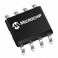
MCP73844-840I/MS Microchip Technology, MCP73844-840I/MS Datasheet - Page 17

MCP73844-840I/MS
Manufacturer Part Number
MCP73844-840I/MS
Description
IC CONTROLLER LI-ION 8.4V 8MSOP
Manufacturer
Microchip Technology
Datasheet
1.MCP73844-840IMS.pdf
(24 pages)
Specifications of MCP73844-840I/MS
Battery Type
Lithium-Ion (Li-Ion), Lithium-Polymer (Li-Pol)
Package / Case
8-TSSOP, 8-MSOP (0.118", 3.00mm Width)
Function
Charge Management
Voltage - Supply
8.7 V ~ 12 V
Operating Temperature
-40°C ~ 85°C
Mounting Type
Surface Mount
Output Voltage
8.442 V
Output Current
10 mA
Operating Supply Voltage
8.7 V to 12 V
Supply Current
4 mA
Maximum Operating Temperature
+ 85 C
Minimum Operating Temperature
- 40 C
Mounting Style
SMD/SMT
Uvlo Start Threshold
8.90 V
Uvlo Stop Threshold
8.85 V
Input Voltage
12V
Battery Charge Voltage
8.4V
Charge Current Max
10mA
Battery Ic Case Style
MSOP
No. Of Pins
8
No. Of Series Cells
2
Rohs Compliant
Yes
Lead Free Status / RoHS Status
Lead free / RoHS Compliant
For Use With
MCP7383XRD-PPM - REFERENCE DESIGN PWR-PTH MCP7383MCP7384XEV - KIT EVALUATION FOR MCP7384X
Lead Free Status / Rohs Status
Lead free / RoHS Compliant
Available stocks
Company
Part Number
Manufacturer
Quantity
Price
Part Number:
MCP73844-840I/MS
Manufacturer:
MICRCOHI
Quantity:
20 000
Worst-case V
and a maximum sink voltage of 1.0V is:
At this worst-case (V
must be low enough as to not impede the performance
of the charging system. The maximum allowable
R
The Fairchild NDS8434 and International Rectifier
IRF7404 both satisfy these requirements.
6.1.1.3
The MCP7384X are stable with or without a battery
load. In order to maintain good AC stability in the
Constant-Voltage mode, a minimum capacitance of
4.7 µF is recommended to bypass the V
This capacitance provides compensation when there is
no battery load. Additionally, the battery and
interconnections appear inductive at high frequencies.
These elements are in the control feedback loop during
Constant-Voltage
capacitance may be necessary to compensate for the
inductive nature of the battery pack.
Virtually any good quality output filter capacitor can be
used, independent of the capacitor’s minimum ESR
(Effective Series Resistance) value. The actual value of
the capacitor and its associated ESR depends on the
forward transconductance (g
external pass transistor. A 4.7 µF tantalum or aluminum
electrolytic capacitor at the output is usually sufficient
to ensure stability for up to a 1A output current.
6.1.1.4
The
depicted in Figure 6-1, provides protection from a
faulted or shorted input, or from a reversed-polarity
input source. Without the protection diode, a faulted or
shorted input would discharge the battery pack through
the body diode of the external pass transistor.
If a reverse-protection diode is incorporated into the
design, it should be chosen to handle the fast charge
current continuously at
temperature. In addition, the reverse-leakage current
of the diode should be kept as small as possible.
2004 Microchip Technology Inc.
R
DSON
DSON
R
V
optional
DSON
GS
at the worst-case V
=
=
EXTERNAL CAPACITORS
REVERSE-BLOCKING PROTECTION
4.5V 120 115 mV
------------------------------------------------------------------------ -
=
1.0V
GS
V
-------------------------------------------------------------------------------
–
reverse-blocking
with a 5V, ±10% input voltage source
DDMIN
–
551 581 mA
mode.
4.5V 120mV
GS
–
) the R
V
–
I
GS
FCSMAX
REGMAX
Therefore,
m
the maximum ambient
is:
) and capacitance of the
–
DSON
4.221V
–
protection
=
V
of the MOSFET
BATMAX
–
3.38V
BAT
=
the
288m
pin to V
bypass
diode,
SS
.
6.1.1.5
In the stand-alone configuration, the enable pin is
generally tied to the input voltage. The MCP7384X
automatically enters a Low-power mode when voltage
on the V
voltage (V
0.4 µA, typically.
6.1.1.6
A status output provides information on the state of
charge. The current-limited, open-drain output can be
used to illuminate an external LED. Refer to Table 5-1
for a summary of the state of the status output during a
charge cycle.
6.2
For optimum voltage regulation, place the battery pack
as close as possible to the device’s V
This is recommended to minimize voltage drops along
the high current-carrying PCB traces.
If the PCB layout is used as a heatsink, adding many
vias around the external pass transistor can help
conduct more heat to the back plane of the PCB, thus
reducing the maximum junction temperature.
DD
PCB Layout Issues
STOP
ENABLE INTERFACE
CHARGE STATUS INTERFACE
input falls below the undervoltage lockout
MCP73841/2/3/4
), reducing the battery drain current to
DS21823C-page 17
BAT
and V
SS
pins.


