LT3650EDD-4.2#PBF Linear Technology, LT3650EDD-4.2#PBF Datasheet
LT3650EDD-4.2#PBF
Specifications of LT3650EDD-4.2#PBF
Available stocks


Related parts for LT3650EDD-4.2#PBF


LT3650EDD-4.2#PBF Summary of contents
Page 1
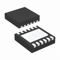
... The LT3650 is available in a low profi le (0.75mm) 3mm × 3mm 12-pin DFN and 12-pin MSOP packages. L, LT, LTC, LTM, Linear Technology and the Linear logo are registered trademarks of Linear Technology Corporation. All other trademarks are the property of their respective owners. ...
Page 2
... T JMAX JA EXPOSED PAD (PIN 13) IS GND, MUST BE SOLDERED TO PCB ORDER INFORMATION LEAD FREE FINISH TAPE AND REEL LT3650EDD-4.1#PBF LT3650EDD-4.1#TRPBF LT3650IDD-4.1#PBF LT3650IDD-4.1#TRPBF LT3650EDD-4.2#PBF LT3650EDD-4.2#TRPBF LT3650IDD-4.2#PBF LT3650IDD-4.2#TRPBF LT3650EMSE-4.1#PBF LT3650EMSE-4.1#TRPBF LT3650IMSE-4.1#PBF LT3650IMSE-4.1#TRPBF LT3650EMSE-4.2#PBF LT3650EMSE-4.2#TRPBF LT3650IMSE-4.2#PBF LT3650IMSE-4.2#TRPBF Consult LTC Marketing for parts specifi ed with wider operating temperature ranges. *The temperature grade is identifi label on the shipping container. ...
Page 3
ELECTRICAL CHARACTERISTICS temperature range, otherwise specifi cations are at V SYMBOL PARAMETER LT3650 V V Operating Range Start Voltage IN V OVLO Threshold IN(OVLO) OVLO Hysteresis V UVLO Threshold IN(UVLO) UVLO Hysteresis V Battery Float Voltage BAT(FLT) ...
Page 4
LT3650-4.1/LT3650-4.2 ELECTRICAL CHARACTERISTICS temperature range, otherwise specifi cations are at V SYMBOL PARAMETER Status Low Voltage CHRG FAULT I Charge/Discharge Current TIMER V Timer Disable Threshold TIMER(DIS) t Full Charge Cycle Timeout TIMER Precondition Timeout Timer Accuracy ...
Page 5
TYPICAL PERFORMANCE CHARACTERISTICS Switch Drive ( BOOST 0.2 0.4 0.6 0.8 1.0 1.2 1.4 1.6 1.8 I (A) SW 365042 ...
Page 6
LT3650-4.1/LT3650-4.2 PIN FUNCTIONS V (Pin 1): Charger Input Supply 4.75V to 32V. V ≥ 7. – BOOST for start-up 85μA after charge termination. VIN CLP (Pin 2): System Current Limit Input. ...
Page 7
PIN FUNCTIONS (full charge current) is the desired soft-start interval (t For this capacitor value follows the relation: RNG/SS = 50μ • RNG The RNG/SS pin is pulled low during fault ...
Page 8
LT3650-4.1/LT3650-4.2 BLOCK DIAGRAM + 125°C – T DIE 0.2V TIMER – + TIMER OSC. RIPPLE COUNTER COUNT RESET COUNT COUNT RESET ENABLE MODE (TIMER OR C/10) CHRG CONTROL LOGIC TERMINATE FAULT SS RESET STATUS C/10 PRECONDITION NTC + – – ...
Page 9
OPERATION OVERVIEW LT3650 is a complete monolithic, mid-power, Li-Ion battery charger, addressing high input voltage applications with solutions that use a minimum of external components. The IC uses a 1MHz constant-frequency, average current mode step-down architecture. Internal reverse-voltage protection allows ...
Page 10
LT3650-4.1/LT3650-4.2 OPERATION The I error voltage corresponds linearly to average TH current sensed across the inductor current sense resistor, allowing maximum charge current control by limiting the effective voltage range clamp limits this voltage TH to ...
Page 11
APPLICATIONS INFORMATION V Input Supply IN The LT3650 is biased directly from the charger input supply through the V pin. This supply provides large IN switched currents high quality, low ESR decoupling capacitor is recommended to minimize voltage ...
Page 12
LT3650-4.1/LT3650-4.2 APPLICATIONS INFORMATION R : Charge Current Programming SENSE The LT3650 charger is confi gurable to charge at average currents as high as 2A. Maximum charge current is set by choosing an inductor sense resistor such that the desired maximum ...
Page 13
... The LT3650 integrates the CLP signal internally, so average ( ) BAT PRE ( ) A current limiting is performed in most cases without the need for external fi lter elements. PowerPath is a trademark of Linear Technology Corporation LT3650 365042 F04 LT3650-4.1/LT3650-4.2 TM control feature to ) such that the desired maximum current ...
Page 14
LT3650-4.1/LT3650-4.2 APPLICATIONS INFORMATION RNG/SS: Dynamic Charge Current Adjust The LT3650 gives the user the capability to adjust maximum charge current dynamically through the RNG/SS pin. The voltage on the RNG/SS pin corresponds to ten times the maximum voltage across the ...
Page 15
APPLICATIONS INFORMATION Status Pins The LT3650 reports charger status through two open-col- lector outputs, the CHRG and FAULT pins. These pins can accept voltages as high and can sink up to 10mA IN when enabled. The CHRG ...
Page 16
LT3650-4.1/LT3650-4.2 APPLICATIONS INFORMATION Preconditioning and Bad-Battery Fault An LT3650 charger has a precondition mode, in which charge current is limited to 15% of the programmed I as set The precondition current corresponds SENSE to 15mV across R ...
Page 17
APPLICATIONS INFORMATION Layout Considerations The LT3650 switch node has rise and fall times that are typically less than 10ns to maximize conversion effi ciency. The switched node (Pin SW) trace should be kept as short as possible to minimize high ...
Page 18
LT3650-4.1/LT3650-4.2 TYPICAL APPLICATIONS 5V to 32V 1.5A Charger with Three Hour EOC Termination. The LTC1515 Provides Boost Start-Up Requirement. Status Pins Use LED Indicators. 2N3904 10k BZX84C6V2L (6.2V) INPUT SUPPLY 5V TO 32V 12V to 32V 2A Charger with Three ...
Page 19
... LEAD COPLANARITY (BOTTOM OF LEADS AFTER FORMING) SHALL BE 0.102mm (.004") MAX Information furnished by Linear Technology Corporation is believed to be accurate and reliable. However, no responsibility is assumed for its use. Linear Technology Corporation makes no representa- tion that the interconnection of its circuits as described herein will not infringe on existing patent rights. ...
Page 20
... Outputs 1- to 4-Cell Li 18-Cell Ni, SLA and Supercap Compatible; 4mm × 4mm QFN-20 Package, LTC4009-1 Version for 4.1V Float Voltage Li-Ion, LTC4009-2 Version for 4.2V Float Voltage Li-Ion Cells. www.linear.com ● B240A 10μH 0.068 + 10μ 3380 10k 365042 TA04 36504142fb LT 0809 REV A • PRINTED IN USA © LINEAR TECHNOLOGY CORPORATION 2009 ...