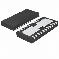
LTC4090EDJC#PBF Linear Technology, LTC4090EDJC#PBF Datasheet - Page 13

LTC4090EDJC#PBF
Manufacturer Part Number
LTC4090EDJC#PBF
Description
IC USB POWER MANAGER 22-DFN
Manufacturer
Linear Technology
Datasheet
1.LTC4090EDJCPBF.pdf
(28 pages)
Specifications of LTC4090EDJC#PBF
Function
Power Management
Battery Type
Lithium-Ion (Li-Ion), Lithium-Polymer (Li-Pol)
Voltage - Supply
4.35 V ~ 5.5 V
Operating Temperature
-40°C ~ 85°C
Mounting Type
Surface Mount
Package / Case
22-WFDFN Exposed Pad
Supply Voltage Range
4.35V To 5.5V
Operating Temperature Range
-40°C To +85°C
Digital Ic Case Style
DFN
No. Of Pins
22
Msl
MSL 1 - Unlimited
Termination Type
SMD
Supply Voltage Min
4.35V
Rohs Compliant
Yes
Filter Terminals
SMD
Frequency
2.7MHz
Lead Free Status / RoHS Status
Lead free / RoHS Compliant
Available stocks
Company
Part Number
Manufacturer
Quantity
Price
OPERATION
USB Input Current Limit
The input current limit and charge control circuits of the
LTC4090/LTC4090-5 are designed to limit input current as
well as control battery charge current as a function of I
OUT drives the external load and the battery charger.
If the combined load at OUT does not exceed the pro-
grammed input current limit, OUT will be connected to IN
through an internal 215mΩ P-channel MOSFET.
If the combined load at OUT exceeds the programmed input
current limit, the battery charger will reduce its charge cur-
rent by the amount necessary to enable the external load
to be satisfi ed while maintaining the programmed input
current. Even if the battery charge current is set to exceed
the allowable USB current, a correctly programmed input
current limit will ensure that the USB specifi cation is never
violated. Furthermore, load current at OUT will always be
prioritized and only excess available current will be used
to charge the battery.
The input current limit, I
following formula:
where V
and R
to ground. For best stability over temperature and time,
1% metal fi lm resistors are recommended.
The programmed battery charge current, I
fi ned as:
Input current, I
current and the OUT pin output current. V
the input current according to the following equation:
In USB applications, the maximum value for R
should be 2.1k. This will prevent the input current from
exceeding 500mA due to LTC4090/LTC4090-5 tolerances
I
I
I
CL
CHG
IN
CLPROG
=I
=
=
CLPROG
⎛
⎝ ⎜
OUT
⎛
⎝ ⎜
R
50,000
CLPROG
R
1000
+I
PROG
is the total resistance from the CLPROG pin
IN
BAT
is the CLPROG pin voltage (typically 1V)
, is equal to the sum of the BAT pin output
=
• V
• V
R
V
PROG
CLPROG
CLPROG
CLPROG
CL
, can be programmed using the
⎞
⎠ ⎟
=
⎞
⎠ ⎟
50,000V
• 1000
=
R
R
PROG
1000V
CLPROG
CLPROG
CHG
will track
, is de-
CLPROG
OUT
.
and quiescent currents. A 2.1k CLPROG resistor will give
a typical current limit of 476mA in high power mode
(when HPWR is high) or 95mA in low power mode (when
HPWR is low).
When SUSP is driven to a logic high, the input power
path is disabled and the ideal diode from BAT to OUT will
supply power to the application.
High Voltage Step Down Regulator
The power delivered from HVIN to HVOUT is controlled by
a constant-frequency, current mode step down regulator.
An external P-channel MOSFET directs this power to OUT
and prevents reverse conduction from OUT to HVOUT (and
ultimately HVIN).
An oscillator, with frequency set by R
fl op, turning on the internal power switch. An amplifi er and
comparator monitor the current fl owing between HVIN and
SW pins, turning the switch off when this current reaches
a level determined by the voltage at V
servos the V
between OUT and BAT (LTC4090). By keeping the voltage
across the battery charger low, effi ciency is optimized be-
cause power lost to the battery charger is minimized and
power available to the external load is maximized. If the
BAT pin voltage is less than approximately 3.3V, then the
error amplifi er will servo the V
HVOUT output voltage of about 3.6V (LTC4090). An active
clamp on the V
is also clamped to the voltage on the HVEN pin; soft-start
is implemented by generating a voltage ramp at the HVEN
pin using an external resistor and capacitor.
The switch driver operates from either the high voltage
input or from the BOOST pin. An external capacitor and
internal diode are used to generate a voltage at the BOOST
pin that is higher than the input supply. This allows the
driver to fully saturate the internal bipolar NPN power
switch for effi cient operation.
To further optimize effi ciency, the high voltage buck regu-
lator automatically switches to Burst Mode
light load situations. Between bursts, all circuitry associated
with controlling the output switch is shut down reducing
the input supply current.
Burst Mode is a registered trademark of Linear Technology Corporation
C
C
node to maintain approximately 300mV
LTC4090/LTC4090-5
node provides current limit. The V
C
node to provide a constant
T
C
, enables an RS fl ip-
. An error amplifi er
®
operation in
13
C
node
4090fc


