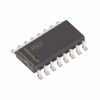
DS2715Z+ Maxim Integrated Products, DS2715Z+ Datasheet - Page 14

DS2715Z+
Manufacturer Part Number
DS2715Z+
Description
IC NIMH CHARGER 16-SOIC
Manufacturer
Maxim Integrated Products
Datasheet
1.DS2715Z.pdf
(17 pages)
Specifications of DS2715Z+
Function
Charge Management
Battery Type
Nickel Metal Hydride (NiMH)
Voltage - Supply
4.5 V ~ 16 V
Operating Temperature
-20°C ~ 85°C
Mounting Type
Surface Mount
Package / Case
16-SOIC (0.154", 3.90mm Width)
Operating Supply Voltage
16.5 V
Supply Current
1.3 mA
Maximum Operating Temperature
+ 85 C
Minimum Operating Temperature
- 20 C
Charge Safety Timers
Yes
Mounting Style
SMD/SMT
Temperature Monitoring
Yes
Uvlo Start Threshold
3.9 V
Uvlo Stop Threshold
35 mV
Lead Free Status / RoHS Status
Lead free / RoHS Compliant
The R
of about 1Ah when charged with the 1.07A charge current. The resistor divider with R12 and R13 is configured to
present the voltage equivalent to a single cell on the Vbatt pin.
The value of L1 in the example represents a moderate switching speed of 100-150khz for fast-charge mode. L1
may be adjusted to fit specific application goals as long as the associated change in switching speed does not
exceed the circuit’s ability to maintain proper regulation of the sense resistor voltage.
PRECHARGE modes have a faster switching frequency than FAST-CHARGE, the regulation in these modes must
be considered.
All capacitors should be ceramic surface mount types of good quality where possible. The 47uF capacitor may be
any type that meets the application requirements. A different network for C1 and C2 may be necessary depending
on the types of capacitors used, the layout, and the transient requirements of the application load. All resistors not
previously mentioned are standard surface mount types.
Linear
Figure 6 shows a typical application circuit for charging a 3-cell stack in linear mode. The Mode pin is tied to V
linear operation. A 250mΩ sense resistor (R7) sets the charge current to .484A, which the DS2715 regulates by
controlling the V
V
CHARGE conditions is 10mA. The RC network of R3 and C5 set a pole in the control loop to ensure stability.
Figure 6. TYPICAL Linear APPLICATION CIRCUIT FOR A 3-CELL STACK
A lower charge current is used for linear mode, in addition to a lower supply voltage. This reduces the power
dissipation of Q1 to a manageable level. This dissipation must be closely considered in the application and proper
heatsinking precautions must be taken. Different transistors may be selected for Q1 based on package size and
thermal requirements. An 86kΩ resistor on R
for the given charge rate is appropriate for cells of about .9Ah capacity. The other aspects of the circuit are
equivalent to those of the switchmode circuit.
CH
+6VDC
is required to sink does not exceed 20mA when V
T
resistor (R5) is set to 47kΩ for a timeout of 70 minutes. This would be appropriate for cells with a capacity
47 uF
C1
GS
B340A-13
of Q1 through the bias resistor R3. The bias resistor should be chosen so that the current that
D1
R7 0.25
1 uF
C2
2N7002
LOAD
Q2
150
.1 uF
R1
C3
10k
R8
LED1
0.1 uF
C4
R5 86K
R4 470
C5 4.7 uF
R3
T
(R5) sets the FAST-CHARGE timeout to about 129 minutes, which
470
LED1
Vdd
Rt
SNS+
Cbias
14 of 17
VSS
Mode
D2
CH
is fully turned on. The preferred design target for FAST-
R2 220
CTG
Vch
IRF9Z24
DS2715
Q1
Vbatt
THM
SNS-
U1
Div
R10
10K
200K
100K
R12
R13
Since TOPOFF and
THM1
10K
SS
for


