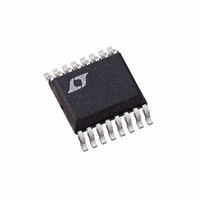
LTC1558CGN-3.3 Linear Technology, LTC1558CGN-3.3 Datasheet - Page 9

LTC1558CGN-3.3
Manufacturer Part Number
LTC1558CGN-3.3
Description
IC BACKUP BATT CNTRLR3.3V 16SSOP
Manufacturer
Linear Technology
Type
Charge Controllerr
Datasheet
1.LTC1558CS8-3.3.pdf
(20 pages)
Specifications of LTC1558CGN-3.3
Function
Back-Up Management
Battery Type
Nickel Cadmium (NiCd)
Voltage - Supply
2.9 V ~ 3.46 V
Operating Temperature
0°C ~ 70°C
Mounting Type
Surface Mount
Package / Case
16-SSOP (0.150", 3.90mm Width)
Output Current
330mA
Output Voltage
1.2V
Operating Supply Voltage (min)
2.9V
Operating Supply Voltage (typ)
3.3V
Operating Supply Voltage (max)
3.465V
Operating Temp Range
0C to 70C
Package Type
SSOP N
Mounting
Surface Mount
Pin Count
16
Operating Temperature Classification
Commercial
Lead Free Status / RoHS Status
Contains lead / RoHS non-compliant
Available stocks
Company
Part Number
Manufacturer
Quantity
Price
Company:
Part Number:
LTC1558CGN-3.3
Manufacturer:
LT
Quantity:
10 000
APPLICATIONS
Once V
converter deactivates and the freshly charged input
capacitor supplies power to the system regulator. The
cycle repeats again when the input capacitor’s charge is
drained away and V
The BACKUP pin remains asserted until the main battery
is restored. This ensures that the LTC1558 does not switch
in and out of backup mode unnecessarily.
The LTC1558’s boost converter minimizes output ripple
under light load conditions by reducing the charge trans-
ferred for the first two consecutive switch cycles. When
V
by connecting the SW pin to ground through an internal
0.5 N-channel MOSFET (N1 in the Block Diagram). The
current through the external 22 H inductor rises linearly
through this switch.
When the switch current reaches an internally preset level
of 165mA, the boost converter connects the SW pin to the
V
the Block Diagram). The inductor current discharges
through P1, charging up the capacitor connected exter-
nally to V
inductor current falls at a rate proportional to the differ-
ence between the backup cell voltage and the output
voltage V
indicating all of its energy has been transferred to the
output capacitor, the LTC1558 looks at the FB pin voltage.
If V
the boost converter shuts off both switches and waits for
V
If V
cycle, the LTC1558 immediately reconnects SW to ground,
repeating the boost cycle. If after two consecutive pulses,
V
the LTC1558 decides that the load is not so light after all,
FB
BAK
FB
FB
FB
FB
falls below (V
to drop below (V
is still not above the boost threshold (V
pin through an internal 2 P-channel MOSFET (P1 in
is still less than (V
has increased above the (V
FB
LIGHT CURRENT MODE
165mA
(PEAK)
BAK
rises above (V
Figure 2. Inductor Current During Switching
BAK
. When the inductor current reaches zero,
(C
IN
REF
of the system regulator, Figure 1). The
U
FB
REF
– 7.5%), the boost operation starts
again drops below (V
REF
INFORMATION
REF
– 7.5%) again.
U
– 7.5%), the LTC1558’s boost
HEAVY CURRENT MODE
– 7.5%) after the first boost
330mA
(PEAK)
REF
W
– 7.5%) threshold,
REF
REF
1558 F02
U
– 7.5%).
– 7.5%),
and doubles the internal inductor charging current limit to
330mA for subsequent cycles. This is high current mode.
By doubling the peak inductor current, each boost cycle
effectively carries four times more energy compared to
low current mode (E = 1/2 • LI
output power. When V
threshold, the LTC1558 stops the boost converter and
resets the internal two pulse counter. The next time V
falls below (V
low current mode for at least two boost cycles. Moderate
or changing loads will cause the LTC1558 to shift between
the two peak inductor current limits, keeping the output in
tight regulation. Near its maximum load capability, the
LTC1558 will stay in 330mA high current mode and the
output voltage V
grammed value.
V
The type of output capacitor and the user programmed
V
efficiency. In most applications, the main V
is primarily determined by the requirements of the main
power supply. Such a capacitor will generally meet the
requirements of the LTC1558. In unusual circumstances
or circuits where the main system regulator’s input ca-
pacitor is located some distance away from the LTC1558,
a local output capacitor may be necessary.
The maximum ripple on the V
ESR voltage drop due to the boost converter’s output
current pulses. The ripple frequency and output duty cycle
is proportional to the inductor discharge time. Given a
fixed inductor value (22 H) and a known peak current
limit, the booster’s discharge time in each boost cycle is
BAK
BAK
Capacitor ESR
value will affect the LTC1558’s output ripple and
ESR RIPPLE
V
LTC1558-3.3/LTC1558-5
REF
BAK
– 7.5%), the boost converter restarts in
BAK
Figure 3. V
DISCHARGE
PERIOD
t
DISCH
FB
will hover around the user pro-
BOOST
CYCLE
exceeds the (V
1
BAK
BAK
2
Ripple
), doubling the available
CHARGE
PERIOD
pin is equal to capacitor
t
CH
REF
– 7.5%) boost
1588 F03
BAK
capacitor
9
FB


