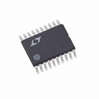
LTC4011CFE#TR Linear Technology, LTC4011CFE#TR Datasheet - Page 9

LTC4011CFE#TR
Manufacturer Part Number
LTC4011CFE#TR
Description
IC BATT CHARGER HIEFF 20TSSOP
Manufacturer
Linear Technology
Datasheet
1.LTC4011CFEPBF.pdf
(26 pages)
Specifications of LTC4011CFE#TR
Function
Charge Management
Battery Type
Nickel Cadmium (NiCd), Nickel Metal-Hydride (NiMH)
Voltage - Supply
4.5 V ~ 34 V
Operating Temperature
0°C ~ 85°C
Mounting Type
Surface Mount
Package / Case
20-TSSOP (0.173", 4.40mm Width) Exposed Pad
Lead Free Status / RoHS Status
Contains lead / RoHS non-compliant
Available stocks
Company
Part Number
Manufacturer
Quantity
Price
pin FuncTions
V
nation. The LTC4011 connects this pin to GND provided the
charger is not in shutdown. V
to GND with an operating voltage range of GND to BAT.
TIMER (Pin 10): Charge Timer Input. A resistor connected
between TIMER and GND programs charge cycle timing
limits. Refer to the Applications Information section for
complete details. Operating voltage range is GND to 1V.
SENSE (Pin 11): Charge Current Sense Input. An external
resistor between this input and BAT is used to program
charge current. Refer to the Applications Information
section for complete details on programming charge
current. Operating voltage ranges from (BAT – 50mV) to
(BAT + 200mV).
BAT (Pin 12): Battery Pack Connection. The LTC4011 uses
the voltage on this pin to control current sourced from
V
voltage range is GND to V
TOC (Pin 13): Active-Low Top-Off Charge Indicator Out-
put. The LTC4011 indicates the top-off charge state for
NiMH batteries by connecting this pin to GND. Refer to
the Operation and Applications Information sections for
further details. This output is capable of driving an LED
and should be left floating if not used. TOC is an open-
drain output to GND with an operating voltage range of
GND to V
INTV
provides a means of bypassing the internal 5V regulator
used to power the BGATE output driver. Typically, power
should not be drawn from this pin by the application
circuit. Refer to the Application Information section for
additional details.
BGATE (Pin 15): External Synchronous N-channel MOSFET
Gate Control Output. This output provides gate drive to
an optional external NMOS power transistor switch used
for synchronous rectification to increase efficiency in the
step-down DC/DC converter. Operating voltage is GND to
INTV
CDIV
CC
to the battery during charging. Allowable operating
DD
DD
(Pin 9): Average Cell Voltage Resistor Divider Termi-
(Pin 14): Internal 5V Regulator Output. This pin
. BGATE should be left floating if not used.
CC
.
CC
.
CDIV
is an open-drain output
PGND (Pin 16): Power Ground. This pin provides a return
for switching currents generated by internal LTC4011 cir-
cuits. Externally, PGND and GND should be wired together
using a very low impedance connection. Refer to PCB
Layout Considerations in the Applications Information
section for additional grounding details.
TGATE (Pin 17): External P-channel MOSFET Gate Control
Output. This output provides gate drive to an external PMOS
power transistor switch used in the DC/DC converter. Op-
erating voltage range varies as a function of V
the Electrical Characteristics table for specific voltages.
V
circuits normally connect either the DC input power sup-
ply or the battery to this pin. Refer to the Applications
Information section for further details. Suggested applied
voltage range is GND to 34V.
READY (Pin 19): Active-Low Ready-to-Charge Output.
The LTC4011 connects this pin to GND if proper operating
voltages for charging are present. Refer to the Operation
section for complete details on charge qualification. This
output is capable of driving an LED and should be left
floating if not used. READY is an open-drain output to
GND with an operating voltage range of GND to V
INFET (Pin 20): PowerPath Control Output. For very low
dropout applications, this output may be used to drive
the gate of an input PMOS pass transistor connected
between the DC input (DCIN) and the raw system supply
rail (V
Maximum operating voltage is V
floating if not used.
Exposed Pad (Pin 21): This pin provides enhanced
thermal properties for the TSSOP . It must be soldered
to the PCB copper ground to obtain optimum thermal
performance.
CC
(Pin 18): Power Input. External PowerPath control
CC
). INFET is internally clamped about 6V below V
CC
. INFET should be left
LTC4011
CC
. Refer to
CC
.
4011fb
CC
.


